High gain read circuit for 3D integrated pixel
a high gain, read circuit technology, applied in the direction of tv system scanning details, radio frequency control devices, television systems, etc., can solve the problems of increasing reducing the dynamic range of image sensors, and reducing the performance properties of these smaller pixels, so as to reduce the capacitance of floating diffusion, reduce the effect of almost all unwanted electrical coupling and minimizing electrical crosstalk
- Summary
- Abstract
- Description
- Claims
- Application Information
AI Technical Summary
Benefits of technology
Problems solved by technology
Method used
Image

Examples
second embodiment
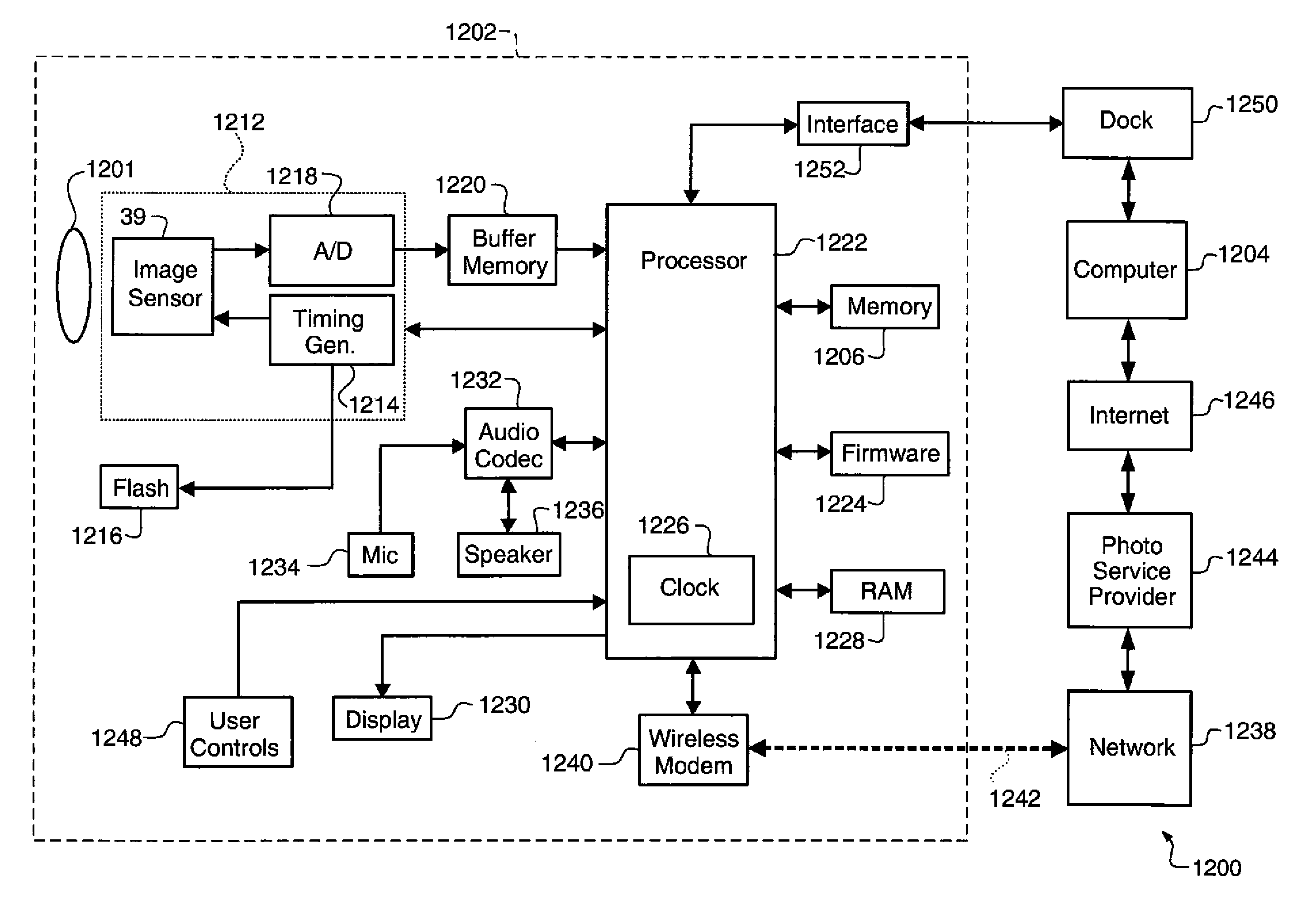
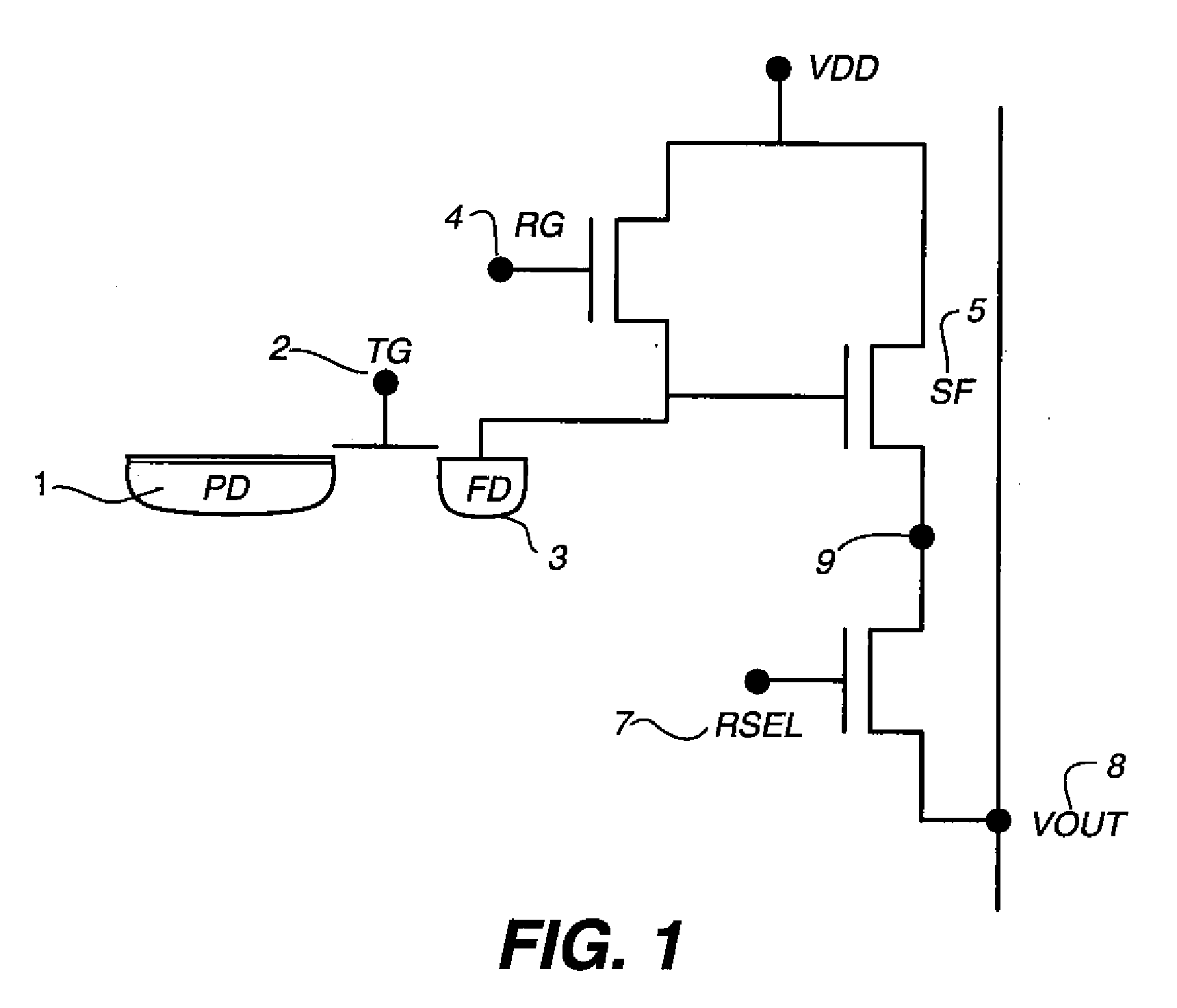
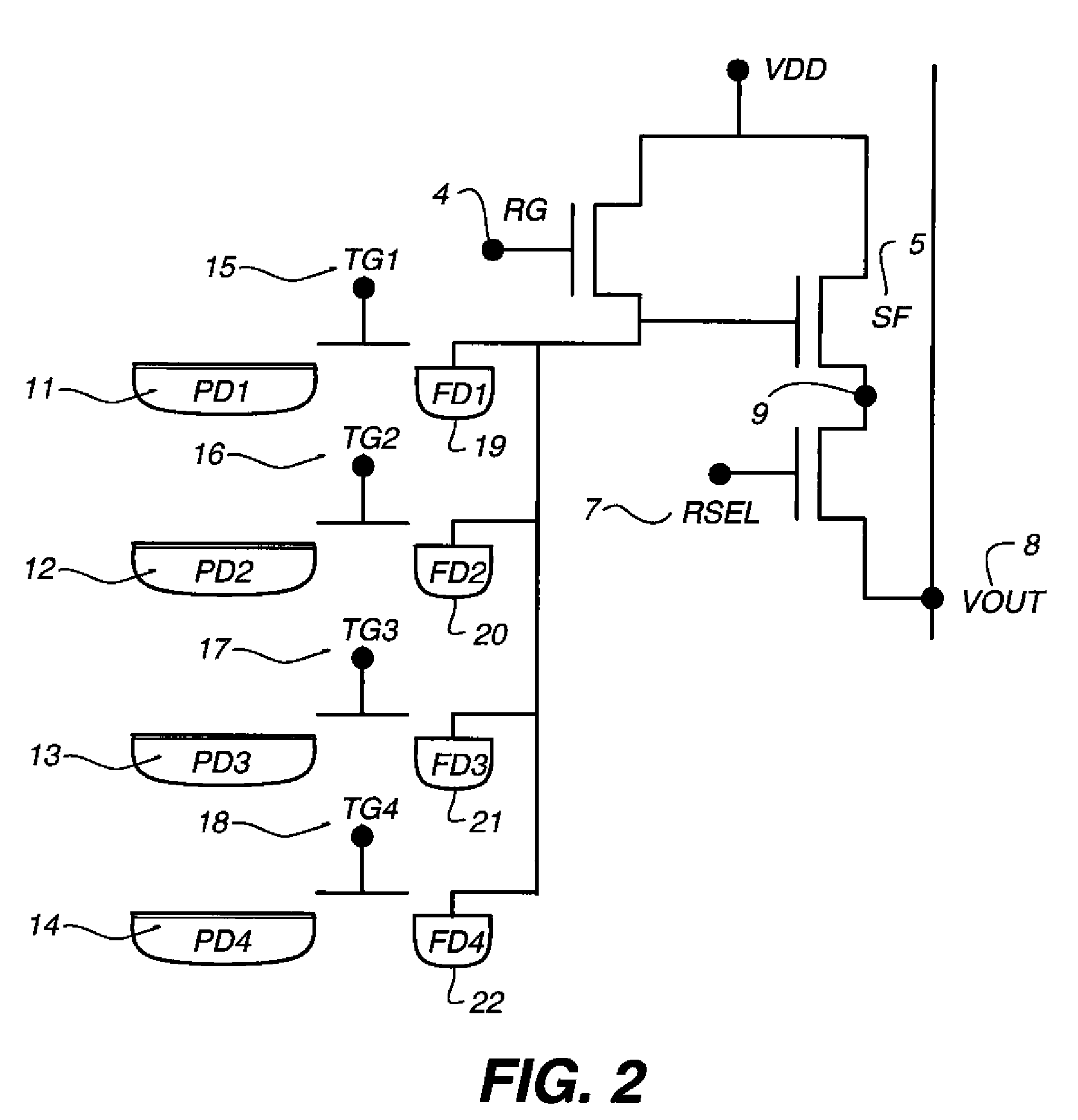
[0028]For most four transistor (4T-pixel) designs, a source follower amplifier, like those shown in FIGS. 1-3, is used to drive the large capacitance of the column circuit. However, the voltage amplification of a source follower circuit is less than one. FIGS. 7 and 8 illustrate a second embodiment that amplifies the voltage applied to the metal shield 100 surrounding the wafer-to-wafer electrical interconnect 68. This reduces the effective capacitance of the floating diffusion 49 and 65. It is noted that this embodiment is the same as FIG. 7 except that a voltage amplifier 120 is attached between the metal shield 100 and the output 109 of the source follower amplifier 105. More specifically, the input of the voltage amplifier 120 is connected to the output 109 of the source follower amplifier 105. Alternatively, the input of the voltage amplifier 120 is connected to the output of the row select transistor 107 (see dashed line). The input voltage to the amplifier 120 needs to be pro...
third embodiment
[0029]FIG. 9 illustrates a This embodiment is the same as FIG. 8 except that a charge pump 111, 140, 141, 142, 143 (the charge pump consists of the elements 111, 140, 141, 142, 143) is substituted for the amplifier 120. Charge pump 111, 140, 141, 142, 143 is small in comparison to other circuits that use operational amplifiers. This provides a gain of greater than 1, and does not require an operational amplifier. The timing for switching transistors phi_1141, phi_2142, and phi_3143 is shown in FIG. 10. When charge is transferred to the floating diffusion 49 and 65, phi_1141 and phi_3143 are on, and phi_2142 off. Assuming the gain of the source follower transistor is 1 then the initial output voltage from the source follower amplifier 105 is QFD / CFD where QFD is the charge on the floating diffusion node, and CFD is the effective floating diffusion capacitance not including the capacitance to the shield. Next, the voltage on the shield is increased using the charge pump. First phi_14...
PUM
 Abstract
Description
Claims
Application Information
 - Generate Ideas
- Intellectual Property
- Life Sciences
- Materials
- Tech Scout
- Unparalleled Data Quality
- Higher Quality Content
- 60% Fewer Hallucinations
Browse by: Latest US Patents, China's latest patents, Technical Efficacy Thesaurus, Application Domain, Technology Topic, Popular Technical Reports.
© 2025 PatSnap. All rights reserved.Legal|Privacy policy|Modern Slavery Act Transparency Statement|Sitemap|About US| Contact US: help@patsnap.com