Chip-on-glass panel device

a technology of glass panel and chip, applied in non-linear optics, instruments, optics, etc., can solve problems such as overheating, circuit damage, explosion,

Active Publication Date: 2010-03-11
HIMAX TECH LTD
View PDF2 Cites 11 Cited by
  • Summary
  • Abstract
  • Description
  • Claims
  • Application Information

AI Technical Summary

Problems solved by technology

Either way, the power lines 361 and 391 are problematic because they usually cause overheating, circuit damage, explosion, and even fire.

Method used


Image

  • Chip-on-glass panel device
  • Chip-on-glass panel device
  • Chip-on-glass panel device

Examples


Embodiment Construction

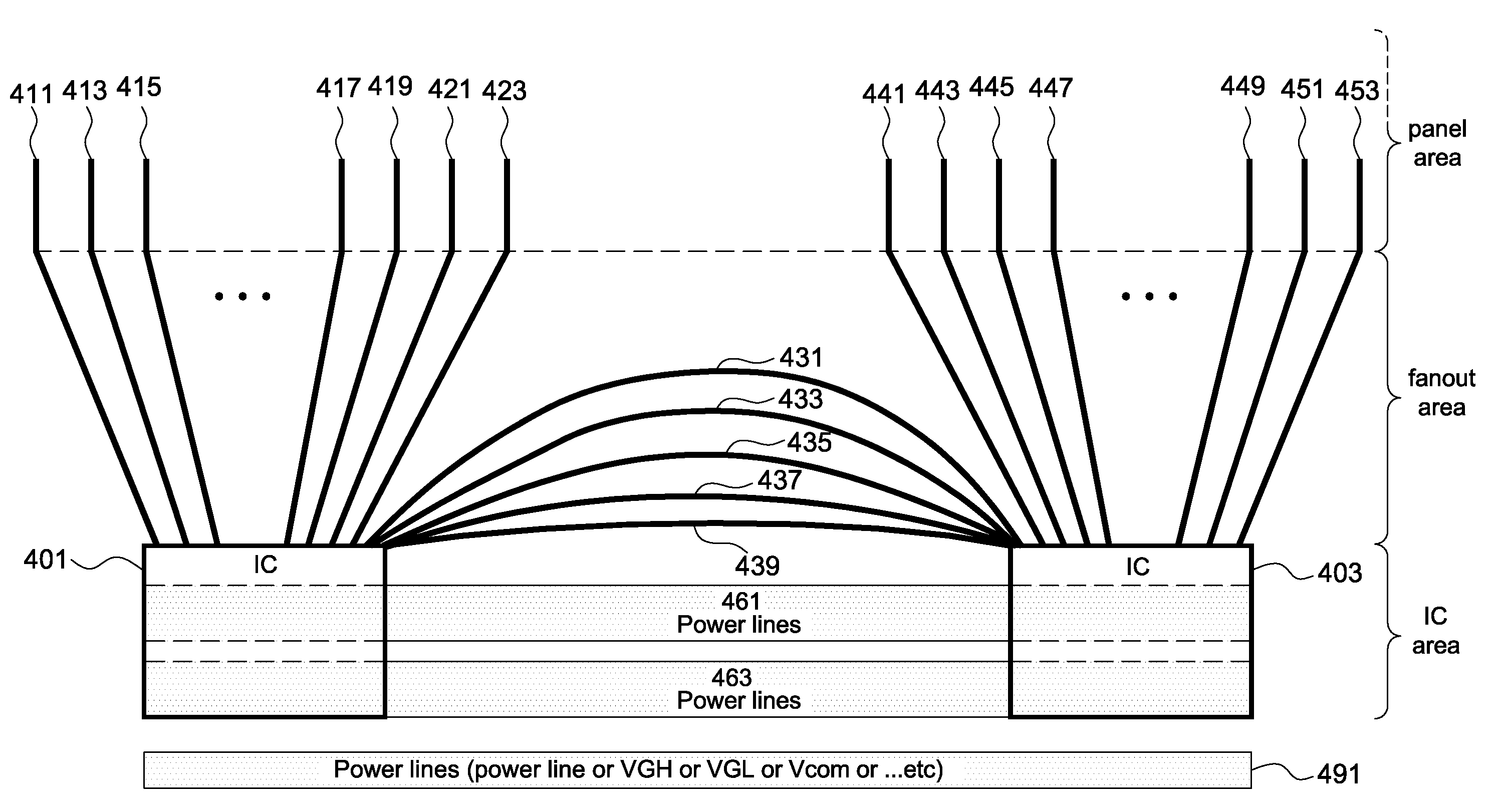
[0021]FIG. 4 is a side view of an exemplary driver circuit layout structure according to one embodiment. In FIG. 4, an exemplary layout structure of a COG panel and pad positions of a drive IC can be configured on a glass substrate (not shown) to form a display, and can include ICs 401 and 403, i.e., source drive ICs. The glass substrate (not shown) can include a display panel area having a plurality of pixels, an IC area for the ICs 401 and 403, and a fan out area between the IC area and the panel display area. The signals wires and gamma wires 431, 433, 435, 437, and 439 can be arranged to have a curved shape geometry disposed in the fan out area.

[0022]FIG. 5 is a plan view of exemplary output pads and signals / gamma pads according to one embodiment. In FIG. 5, an active surface of the IC 401 or 403 (in FIG. 4) can be arranged to include a plurality of output pads 531 to 559, signal pads / gamma pads 501 to 509 and 571 to 579 on the active surface. The output pads 531 to 559 can be c...


PUM

PropertyMeasurementUnit
areaaaaaaaaaaa
flexibleaaaaaaaaaa
light transmittanceaaaaaaaaaa

Abstract

A chip-on-glass panel device includes a glass substrate having a pixel area, an integrated circuit area, and a fan out area, the fan out area located between the pixel area and the IC area, a plurality of integrated circuit devices arranged within the integrated area of the glass substrate, each of the plurality of integrated circuit devices havean active surface, a plurality of output pads, each arranged on the active surface, and a plurality of signal pads / gamma pads, each arranged on the active surface, and a plurality of signal wires / gamma wires, each having a curved shape geometry and disposed within the fan out area, for connecting the plurality of signal pads / gamma pads of adjacent ones of the plurality of integrated circuit devices through the fan out area.

Description

BACKGROUND[0001]1. Technical Field[0002]The embodiments described herein generally relate to a layout structure, and more particularly to a circuit layout structure of a display.[0003]2. Related Art[0004]Generally, a liquid crystal display (LCD) device controls light transmittance through a liquid crystal material having a dielectric anisotropy by adjusting an electric field (to display images). The LCD device includes a LCD panel for displaying the images, and a driving circuit for driving pixel cells of the LCD panel. The driving circuit includes a gate driver for driving gate lines of the LCD panel, a source driver for driving the data lines, a timing controller for controlling drive timing of the gate driver and the source driver, and a power supply for supplying power signals required for driving the LCD panel and the driving circuit.[0005]The source driver and the gate driver are separated into a plurality of integrated circuits (ICs) that are manufactured as semiconductor chi...

Claims


Application Information

Patent Timeline
Patent Type & Authority Applications(United States)
IPC IPC(8): G02F1/1345
CPCG02F1/13454G02F1/1345
Inventor KU, TZONG-YAU
Owner HIMAX TECH LTD
Why Eureka
Try Eureka