Photoelectric conversion device and imaging system

a conversion device and photoelectric technology, applied in the field of photoelectric conversion devices and imaging systems, can solve problems such as the difficulty of ensuring the contact area between color filters and insulation films

Inactive Publication Date: 2010-03-18
CANON KK
View PDF11 Cites 23 Cited by
  • Summary
  • Abstract
  • Description
  • Claims
  • Application Information

AI Technical Summary

Benefits of technology

[0009]The present invention provides for preventing a plurality of color filters from peeling from an insulation film even w...

Problems solved by technology

In this case, it is difficult to ensure the contact...

Method used


Image

  • Photoelectric conversion device and imaging system
  • Photoelectric conversion device and imaging system
  • Photoelectric conversion device and imaging system

Examples


first embodiment

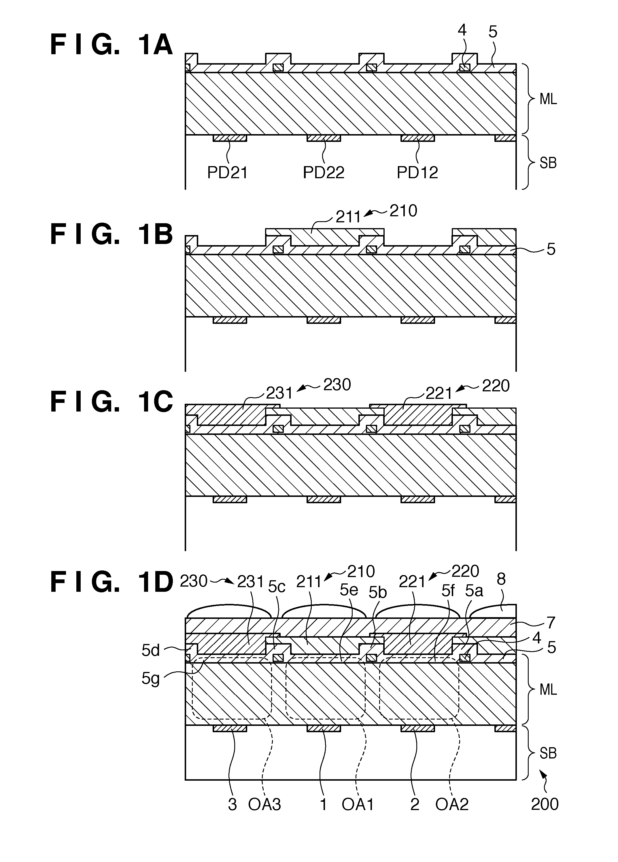
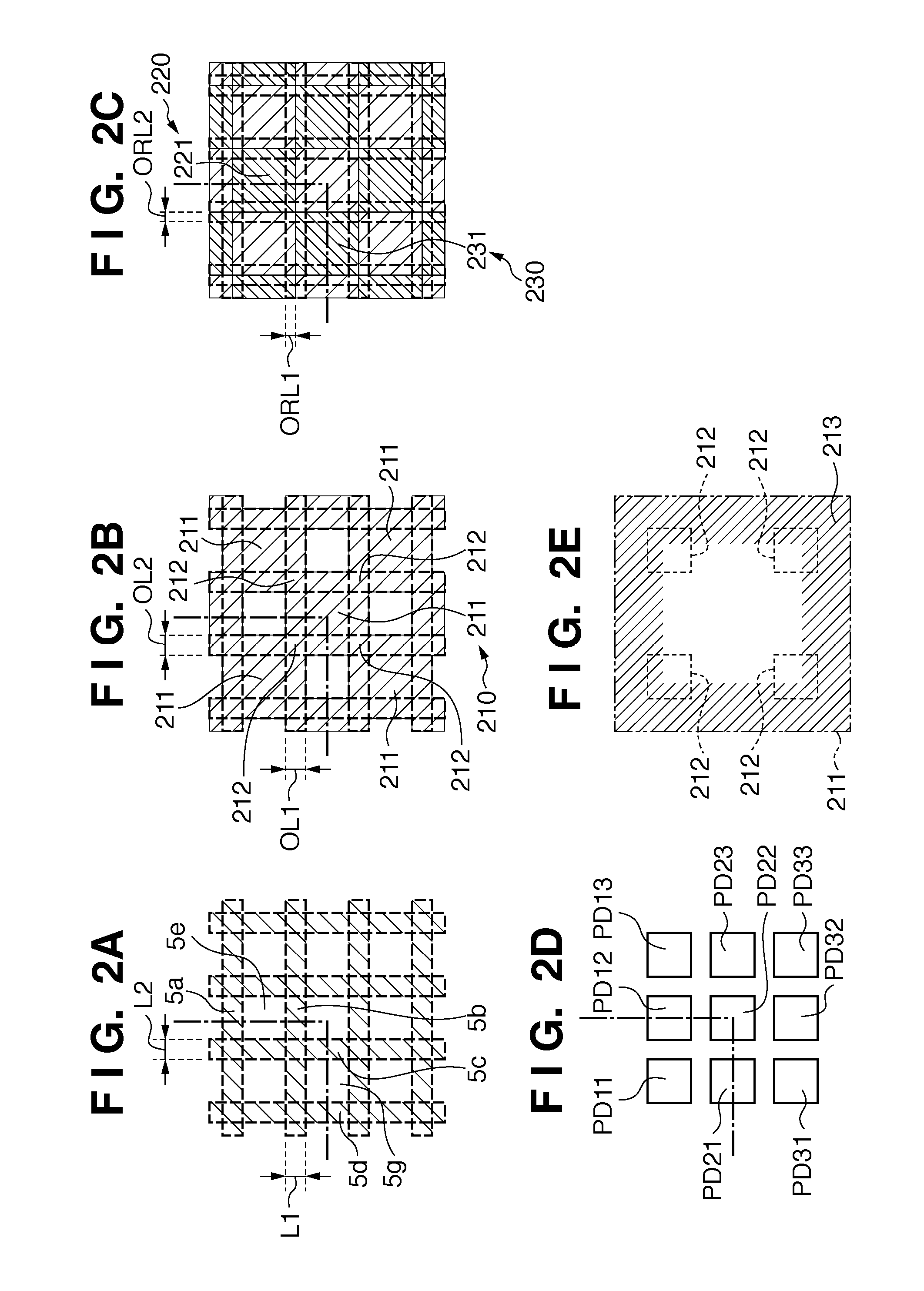
[0022]A problem to be solved by the present invention will be explained with reference to FIGS. 8 and 2D. FIG. 8 is a sectional view showing sectional structures of a photoelectric conversion device 100. FIG. 2D is a plan view for explaining a layout of photoelectric conversion units in the This layout is also applied to a plurality of photoelectric conversion units in the photoelectric conversion device 100, and will be used to explain the layout of photoelectric conversion units in the photoelectric conversion device 100.

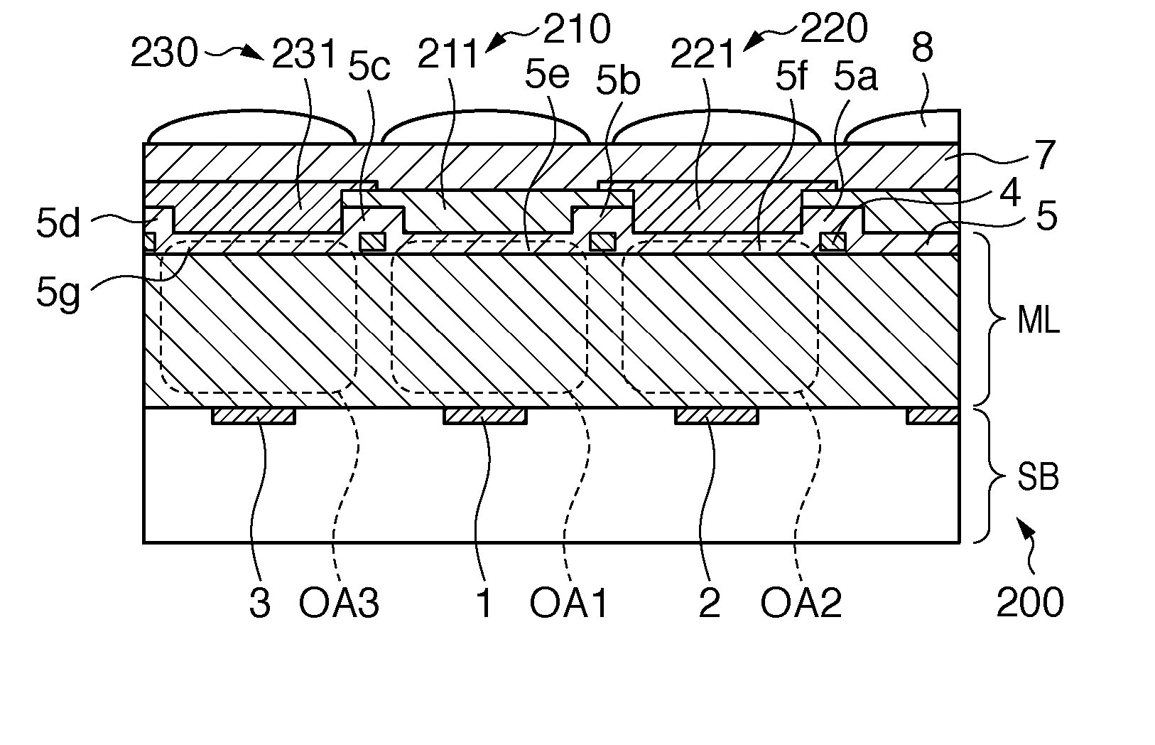
[0023]The photoelectric conversion device 100 shown in FIG. 8 includes a semiconductor substrate SB, a multilayer wiring structure ML, a first color filter layer 10, a second color filter layer 20, a third color filter layer 30, a planarized film 7, and a plurality of microlenses 8.

[0024]In the semiconductor substrate SB, a plurality of photoelectric conversion units PD11 to PD33 are arrayed in directions along a row and a column (see FIG. 2D). The photoelectric ...

second embodiment

[0085]As shown in FIG. 6B, A represents a length corresponding to ½ of the width of the convex portion of the insulation film 5. The pattern of the third color filter 331 in the second embodiment is etched to remove an isosceles right triangle having a base and opposite side of a length B which is double the length A. As a result, the pattern of the third color filter 331i having the oblique corner portion 331i1 can be obtained.

[0086]The structure of a photoelectric conversion device 400 according to the third embodiment of the present invention will be described with reference to FIGS. 7A to 7C. FIGS. 7A to 7C are plan views showing layouts of color filters in the photoelectric conversion device 400 according to the third embodiment of the present invention. FIG. 7A is a plan view showing concave and convex portions when an insulation film covers an uppermost wiring layer. FIG. 7B is a plan view showing a layout when first color filters are arranged. FIG. 7C is a plan view showing ...


PUM


Abstract

A photoelectric conversion device comprises a semiconductor substrate; a multilayer wiring structure; a first color filter layer including a plurality of first color filters which are arranged above a first photoelectric conversion units to allow light of a first color to enter the first photoelectric conversion units, each first color filter being connected to an adjacent first color filter; and a second color filter layer including a plurality of second color filters which are arranged above a second photoelectric conversion units to allow light of a second color to enter the second photoelectric conversion units, wherein the multilayer wiring structure including an uppermost wiring layer which defines the aperture regions corresponding to the respective photoelectric conversion units, and an insulation film arranged to cover the uppermost wiring layer, and wherein the first color filter layer and the second color filter layer are arranged to cover the insulation film.

Description

BACKGROUND OF THE INVENTION[0001]1. Field of the Invention[0002]The present invention relates to a photoelectric conversion device and imaging system.[0003]2. Description of the Related Art[0004]CMOS photoelectric conversion devices can read out signals at high speed with low noise and are used in digital still cameras, digital video cameras, and the like.[0005]Photoelectric conversion devices require higher resolutions to sense images by decreasing the pixel pitch and increasing the pixel count. At the same time, photoelectric conversion devices need to decrease the distance from a microlens to the light receiving surface of a photodiode so that a lens with a larger optical aperture value, that is a smaller F-number, is available even at a smaller pixel pitch.[0006]According to Japanese Patent Laid-Open No. 2005-328066, red (R), green (G), and blue (B) color filters 19 are formed on a fifth insulation film 18 covering a fourth metal interconnection M4 serving as an uppermost metal ...

Claims


Application Information

Patent Timeline
IPC IPC(8): H04N5/335H01L31/0232H01L31/0216H01L27/14H04N9/07
CPCH01L27/14621H01L27/14627H04N5/2254H01L27/14685H01L27/14636H04N25/134
Inventor KURIHARA, MASAKI
Owner CANON KK
Why Eureka
Try Eureka