Optical element, optical element wafer, optical element wafer module, optical element module, method for manufacturing optical element module, electronic element wafer module, method for manufacturing electronic element module, electronic element module and electronic information device

a technology for optical elements and optical elements, applied in the field of optical elements, can solve problems such as inability to achieve optical characteristics, and achieve the effects of low manufacturing cost, suitable optical characteristics, and low manufacturing cos

Active Publication Date: 2010-03-25
SHARP KK
View PDF9 Cites 76 Cited by
  • Summary
  • Abstract
  • Description
  • Claims
  • Application Information

AI Technical Summary

Benefits of technology

[0066]According to the present invention, in an optical element module, an adhesive is provided only in a space portion surrounded by upper and lower bottom portions provided with upper and lower tapered sections interposed therebetween on a further outer circumference side of each planarized surface of a spacer section of an upper optical element and a spacer section of a lower optical element, so as to adhere the upper optical element and the lower optical element. Thus, the adhesive is provided only in the space portion made by the upper and lower bottom portions, and the adhesive is at least not provided in a space portion made by upper and lower tapered sections. A sufficient space is provided in the space portion made at least by the upper and lower tapered sections so that the adhesive can be pressed and spread by the upper and lower optical elements, yet will not be spread to the spacer section, when adhering. As a result, the adhesive will not be put between the upper and lower spacer sections and the upper and lower spacer sections are indirect contact with each other, and the lens spacing will be stabilized and the optical characteristics will be suitable.
[0067]Further, in an electronic element module, in addition to the structure described above, an adhesive is provided only in a space portion, surrounded by a bottom portion and a transparent support substrate, the bottom portion provided with a tapered section interposed therebetween, on a further outer circumference side of a planarized surface of the spacer section of the lower most optical element, so as to adhere the lower most optical element and the transparent support substrate. Thus, the adhesive is provided only in the space portion made by the bottom portion, but the adhesive is at least not provided in the space portion made by the tapered section, and at least the space portion made by the tapered section includes a space large enough for the adhesive to be pressed and spread by the lowermost optical element and the transparent support substrate, yet not be spread to the spacer section, when adhering. As a result, since there will be no interposition of the adhesive in the spacer section as done conventionally, there will be no variation in the lens space or the space between the lens and the image capturing element, thereby stabilizing the lens space or the space between the lens and the image capturing element and making the optical characteristics suitable.
[0068]According to the present invention with the structure described above, the adhesive is provided only in the space portion surrounded by the bottom portion provided with the tapered section interposed therebetween on the further outer circumference side of the planarized surface of the spacer section of the optical element, but the adhesive is at least not provided in the space portion made by the tapered section. When adhering, a space large enough for the adhesive to be pressed and spread is provided at least by the space portion made by the tapered section. As a result, since the overall thickness is not negatively influenced due to the interposition of the adhesive, which is negatively influenced conventionally, the lens space or the space between the lens and the image capturing element will be stabilized without variations therebetween, and the optical characteristics will be suitable. Furthermore, since there is no change from the conventional cutting process, the manufacturing cost can remain low.

Problems solved by technology

According to the structure of Reference 3, an adhesive 305 is filled in a space portion made by a step portion on the further outside of a contacting surface P, the contacting surface P determining the lens space b. Although the adhesive 305 adheres the substrates 302 and 304, if the amount of the adhesive 305 is too much, the adhesive 305 spreads from the space portion into the contacting surface P, which creates a gap in the contacting surface P. This will create a variation of lens spacing and results in unstable optical characteristics.

Method used


Image

  • Optical element, optical element wafer, optical element wafer module, optical element module, method for manufacturing optical element module, electronic element wafer module, method for manufacturing electronic element module, electronic element module and electronic information device
  • Optical element, optical element wafer, optical element wafer module, optical element module, method for manufacturing optical element module, electronic element wafer module, method for manufacturing electronic element module, electronic element module and electronic information device
  • Optical element, optical element wafer, optical element wafer module, optical element module, method for manufacturing optical element module, electronic element wafer module, method for manufacturing electronic element module, electronic element module and electronic information device

Examples


embodiment 1

[0190]FIG. 1 is an essential part longitudinal cross sectional view illustrating an exemplary unitary structure of an electronic element wafer module according to Embodiment 1 of the present invention.

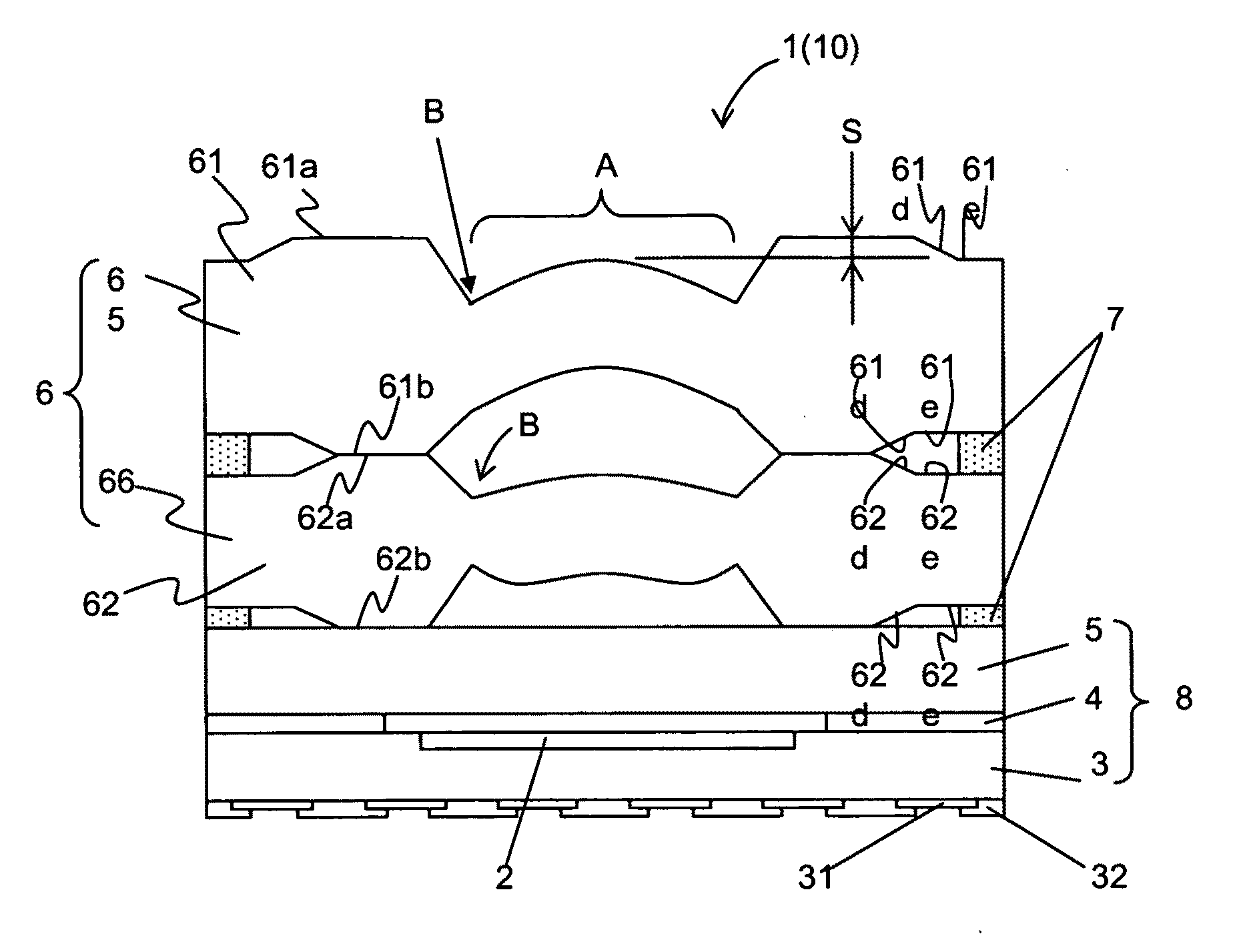
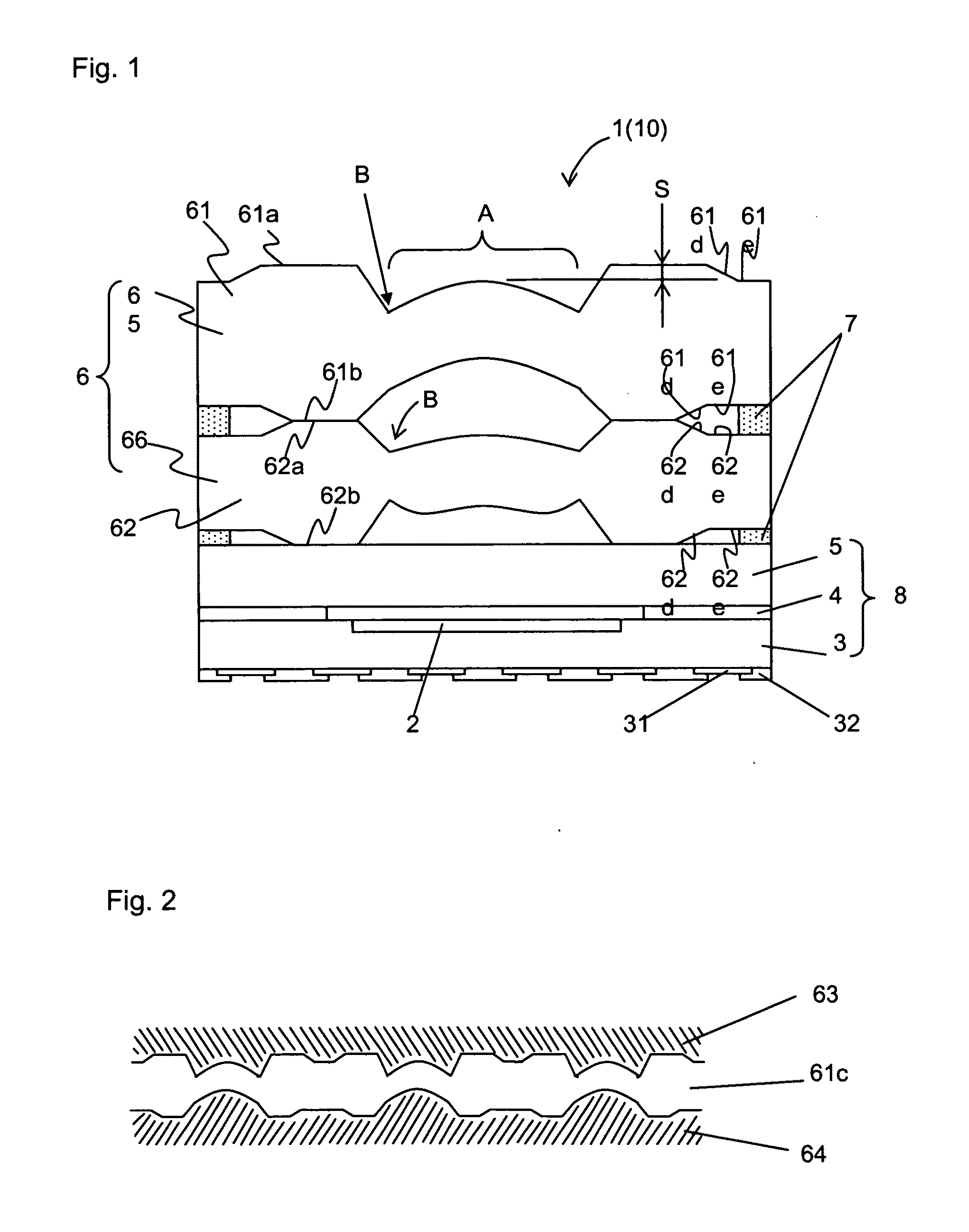
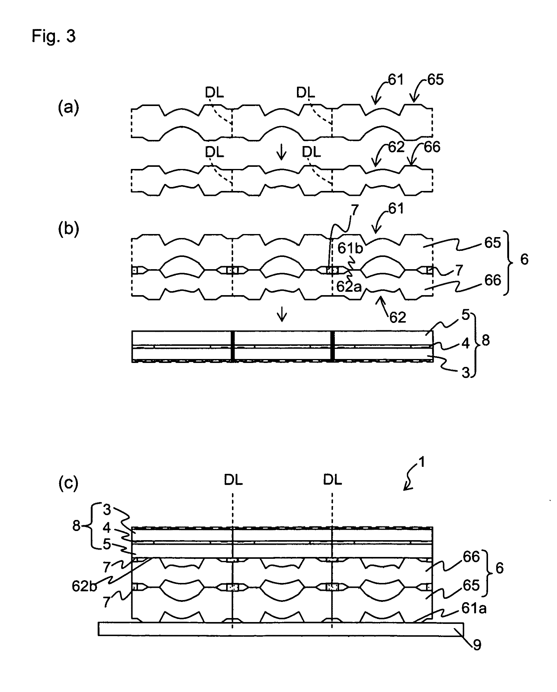
[0191]In FIG. 1, an image capturing element wafer module 1, which functions as an electronic element wafer module according to Embodiment 1, includes: an image capturing element wafer 3 as an electronic element wafer in which a plurality of image capturing elements 2 are arranged in a matrix, the image capturing elements 2 including a plurality of light receiving sections for performing a photoelectric conversion on and capturing an image of image light from a subject; a resin adhesion layer 4 formed on the image capturing element wafer 3 and in between adjacent image capturing elements 2; a transparent support substrate 5, such as a glass plate, adhered and fixed on the resin adhesion layer 4; and a lens wafer module 6, as an optical element wafer module, provided such that lens posit...

embodiment 2

[0234]FIG. 8 is an essential part longitudinal cross sectional view illustrating an exemplary unitary structure of an electronic element wafer module according to Embodiment 2 of the present invention.

[0235]In FIG. 8, an image capturing element wafer module 1B as the electronic element wafer module of Embodiment 2 includes: a plurality of image capturing elements 2 arranged in a matrix, the image capturing elements 2 including a plurality of light receiving sections for performing a photoelectric conversion on and capturing an image of image light from a subject; an image capturing element wafer 3, as an electronic element wafer, in which a penetrating electrode is provided for each image capturing element 2; a resin adhesion layer 4 formed on the image capturing element wafer 3 and in between adjacent image capturing elements 2; a transparent support substrate 5, such as a glass plate, adhered and fixed on the resin adhesion layer 4; and a lens wafer module 6B, as an optical elemen...

embodiment 3

[0270]In Embodiment 3, the lens as an optical element and the lens module as an optical element module will be described in detail.

[0271]FIG. 14(a) is a longitudinal cross sectional view illustrating an exemplary variation of each lens of FIG. 5(c). FIG. 14(b) is a longitudinal cross sectional view illustrating an exemplary variation of the lens module of FIG. 4(b). FIG. 14(c) is a top view of the first lens 61 of FIG. 5(c). FIG. 14(d) is a top view of the first lens of FIG. 14(a). FIG. 14(e) is a longitudinal cross sectional view of a lens module in which the first lens of FIG. 14(a) is combined with the light shielding holder. FIG. 14(f) is a longitudinal cross sectional view of a lens module in which the exemplary variation of the lens module of FIG. 14(b) is combined with the light shielding holder.

[0272]Similar to the case with the FIG. 5(a) and FIG. 5(b), it is possible to obtain a large number of first lenses 84 as well as second lenses 85 as illustrated in FIG. 14(a) by cutt...


PUM

PropertyMeasurementUnit
surface heightaaaaaaaaaa

Abstract

An optical element according to the present invention includes: an optical surface at a center portion thereof; and a spacer section having a predetermined thickness on an outer circumference side of the optical surface, wherein a bottom portion for positioning an adhesive is provided on a further outer circumference side of the spacer section with a tapered portion interposed therebetween.

Description

[0001]This nonprovisional application claims priority under 35 U.S.C. §119(a) to Patent Applications No. 2008-246968 filed in Japan on Sep. 25, 2008, and No. 2009-199049 filed in Japan on Aug. 28, 2009, the entire contents of which are hereby incorporated by reference.BACKGROUND OF THE INVENTION[0002]1. Field of the Invention[0003]The present invention is related to an optical element provided with a lens and an optical function element. Further, the present invention is related to an optical element wafer provided with a plurality of optical elements, such as a plurality of lenses and a plurality of optical function elements, in a wafer state. Further, the present invention is related to an optical element wafer module in which the plurality of optical element wafers are laminated. Further, the present invention is related to an optical element module, which is made by cutting the optical element wafer or the optical element wafer module, and a method for manufacturing the optical ...

Claims


Application Information

Patent Timeline
Patent Type & Authority Applications(United States)
IPC IPC(8): H04N5/335B32B38/10G02B7/02H01L31/12B26D7/08G02B13/00G02B13/18H01L27/14
CPCG02B3/0056H01L27/14685Y10T156/1062G02B13/0085B29D11/00432G02B3/0068H01L31/0232G02B13/003H01L27/14625H01L31/02325Y10T83/0405
Inventor YANO, YUJIHIRANO, KENJI
Owner SHARP KK
Why Eureka
Try Eureka