
Method for manufacturing array substrate of liquid crystal display

a technology of array substrates and liquid crystal displays, which is applied in the direction of optics, semiconductor devices, instruments, etc., can solve the problems of difficult control of etching degree, over-etching of tft channels, and poor display quality of liquid crystal displays, so as to ensure the display quality of liquid crystals and reduce over-etching on tft channels

Active Publication Date: 2010-03-25
BEIJING BOE OPTOELECTRONCIS TECH CO LTD +1
View PDF6 Cites 18 Cited by
  • Summary
  • Abstract
  • Description
  • Claims
  • Application Information

AI Technical Summary

Benefits of technology

[0025]The object of the invention is to provide a method for manufacturing an array substrate of liquid crystal display, so that the over-etching on the TFT channel can be reduced and the display quality of the liquid crystal can be ensured.
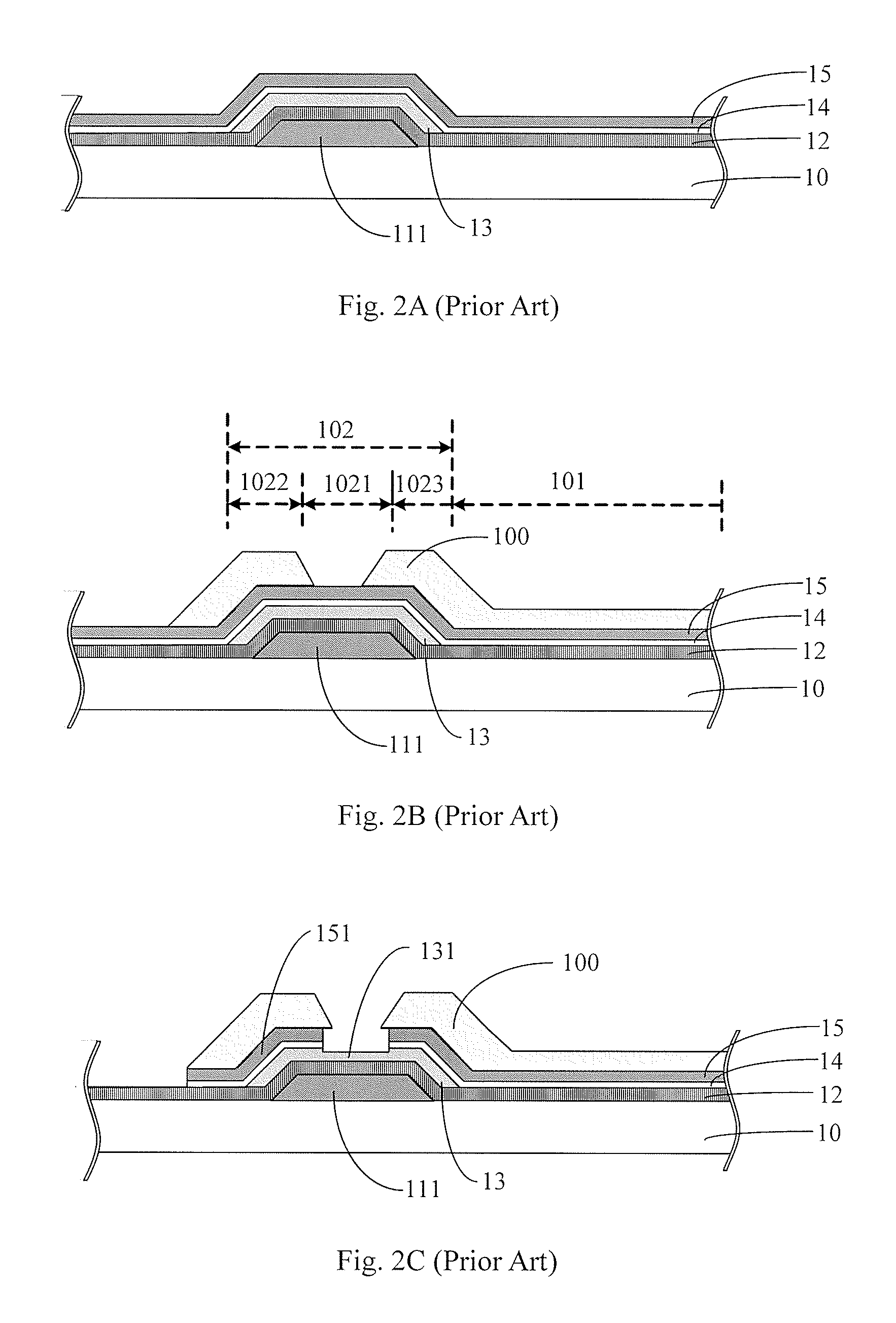
[0044]According to the invention, the photoresist pattern layer is also formed on the TFT channel region through a triple-tone mask so that the TFT channel region is protected when the first wet-etching process is carried out, and then the TFT channel is formed by the dry-etching process capable of accurately controlling the degree of etching. In this way, the TFT channel is subject to one dry-etching process and one wet-etching process in the present invention while it is conventionally subject to two wet-etching processes. Since the number of wet-etching processes performed on the TFT channel is decreased, the over-etching can be reduced and thus the display quality degradation of the liquid crystal display due to excessive wide TFT channel can be avoided.

Problems solved by technology

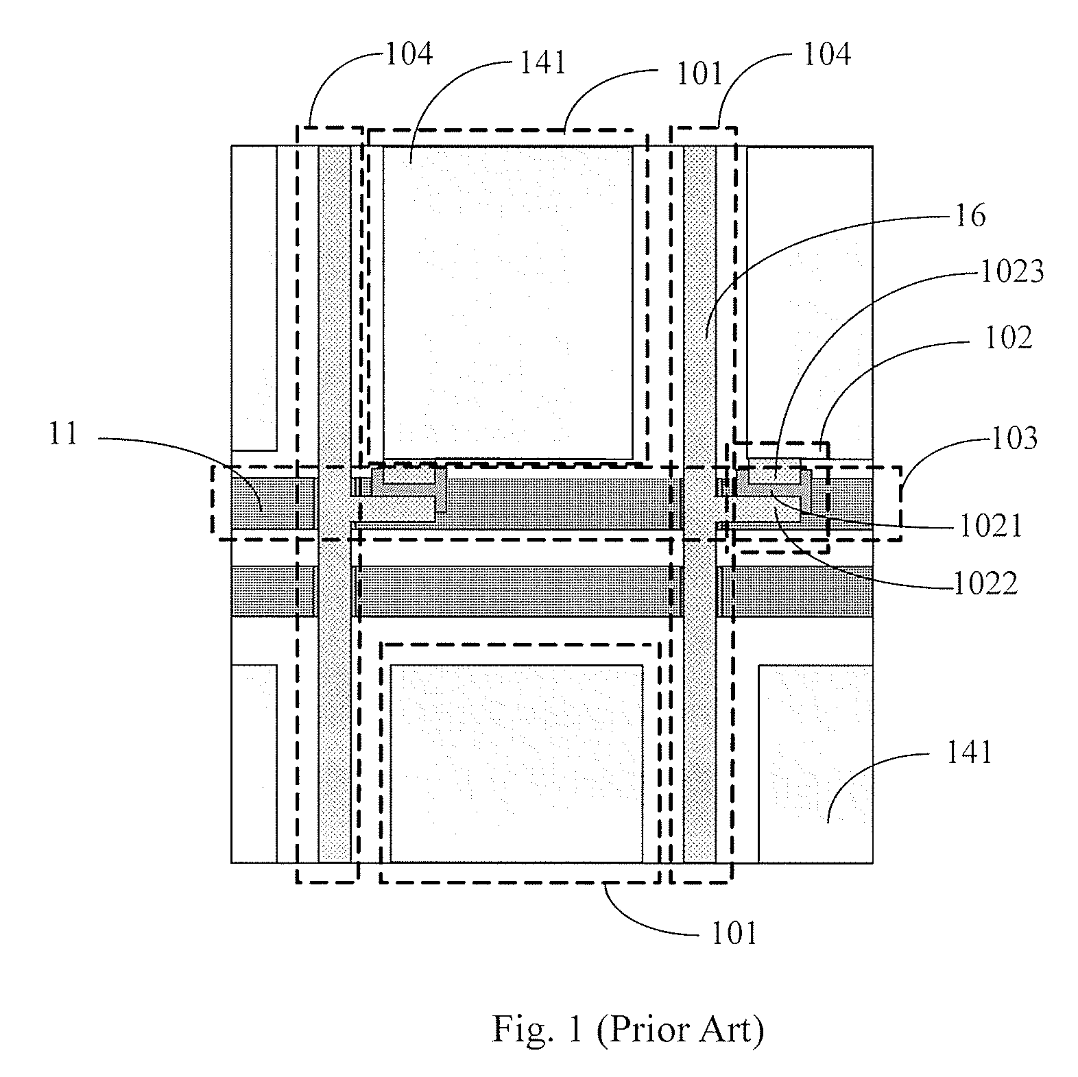
However, it is found that the display quality of liquid crystal display may suffer by using the above methods, which will be described in detail as follows.
Since the TFT channel region is wet-etched twice in the above method and it is difficult to control the degree of etching in the wet-etching process, the problem of over-etching the TFT channel occurs.

Method used


Image

  • Method for manufacturing array substrate of liquid crystal display
  • Method for manufacturing array substrate of liquid crystal display
  • Method for manufacturing array substrate of liquid crystal display

Examples


Embodiment Construction

[0065]FIG. 3 is a flow chart showing a method for manufacturing an array substrate of liquid crystal display according to an embodiment of the invention. Specifically, the method for manufacturing an array substrate of liquid crystal display in the invention can comprise the following steps:

[0066]a. providing a substrate formed with a gate line with integrated gate electrode , a gate insulating layer and an active layer pattern in this order;

[0067]b. depositing a first transparent conductive layer and a source / drain metal layer in this order on the substrate;

[0068]c. forming a photoresist pattern layer on the source / drain metal layer through a triple-tone mask;

[0069]d. performing a wet-etching process on the source / drain metal layer and the first transparent conductive layer exposed from the photoresist pattern layer;

[0070]e. performing a first ashing process on the photoresist pattern layer and performing a dry-etching process on the source / drain metal layer, the first transparent ...


PUM


Abstract

A method for manufacturing an array substrate of liquid crystal display comprising the following steps: providing a substrate having gate lines, a gate insulating layer and an active layer pattern formed thereon in this order; depositing a first transparent conductive layer and a source / drain metal layer in this order on the substrate; forming a photoresist pattern layer on the source / drain metal layer through a triple-tone mask; performing a wet-etching process on the source / drain metal layer and the first transparent conductive layer exposed from the photoresist pattern layer; performing a first ashing process on the photoresist pattern layer and performing a dry-etching process on the source / drain metal layer, the first transparent conductive layer and the active layer pattern exposed by the first ashing process; performing a second ashing process on the photoresist pattern layer and performing a wet-etching process on the source / drain metal layer exposed by the second ashing process; and removing the remaining photoresist pattern layer. According to the invention, the over-etching on the TFT channel region can be reduced and the display quality of the liquid crystal display can be ensured.

Description

BACKGROUND[0001]Embodiments of the present invention relate to a method for manufacturing an array substrate of liquid crystal display, and more particularly to a method for manufacturing an array substrate of liquid crystal display capable of reducing the over-etching.[0002]Nowadays, an array substrate of liquid crystal display panel is typically manufactured by photolithographic process and since the mask employed by the photolithographic process is expensive, reducing the number of the masks to be used is a key for reducing the cost and enhancing the competitive ability.[0003]Several methods have been proposed for reducing the number of the masks employed in the photolithographic process. For example, there is proposed a method in which the transparent electrode (formed by ITO, IZO and the like), the source electrode, the drain electrode and the thin film transistor (TFT) channel are formed through a dual tone mask. The method can be applied to manufacture array substrates for th...

Claims


Application Information

Patent Timeline
IPC IPC(8): H01L21/28
CPCG02F1/1368H01L27/1288H01L27/1214G02F1/136G02F1/13
Inventor CHOI, SEUNGJINSONG, YOUNGSUKYOO, SEONGYEOL
Owner BEIJING BOE OPTOELECTRONCIS TECH CO LTD
Learn More