Systems and methods for implementing a wafer level hermetic interface chip

Inactive Publication Date: 2010-04-08
HONEYWELL INT INC
View PDF9 Cites 18 Cited by
  • Summary
  • Abstract
  • Description
  • Claims
  • Application Information

AI Technical Summary

Benefits of technology

[0010]As will be readily appreciated from the foregoing summary, the invention provides for fabrication of a robust MEMS device that can be hermetically sealed

Problems solved by technology

PLS can lead to problematic effects such as stiction between a sensing wafer and substrate components during a bonding process and lower production yield of MEMS devices.
In practice, WLP design is difficult to implement due to higher non-recurring engineering costs, increased unit production costs, and various technological challenges associated with presently available WLP techniques.
Also, WLP production quantities are usually not high enough to be econom

Method used


Image

  • Systems and methods for implementing a wafer level hermetic interface chip
  • Systems and methods for implementing a wafer level hermetic interface chip
  • Systems and methods for implementing a wafer level hermetic interface chip

Examples


Example

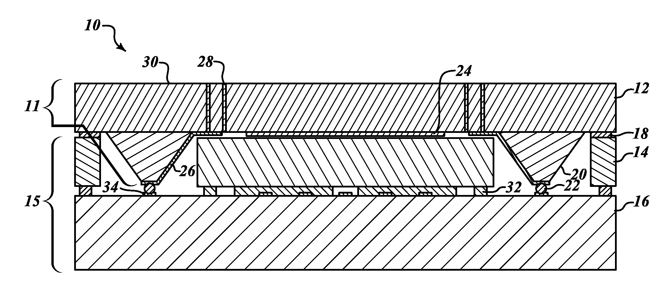
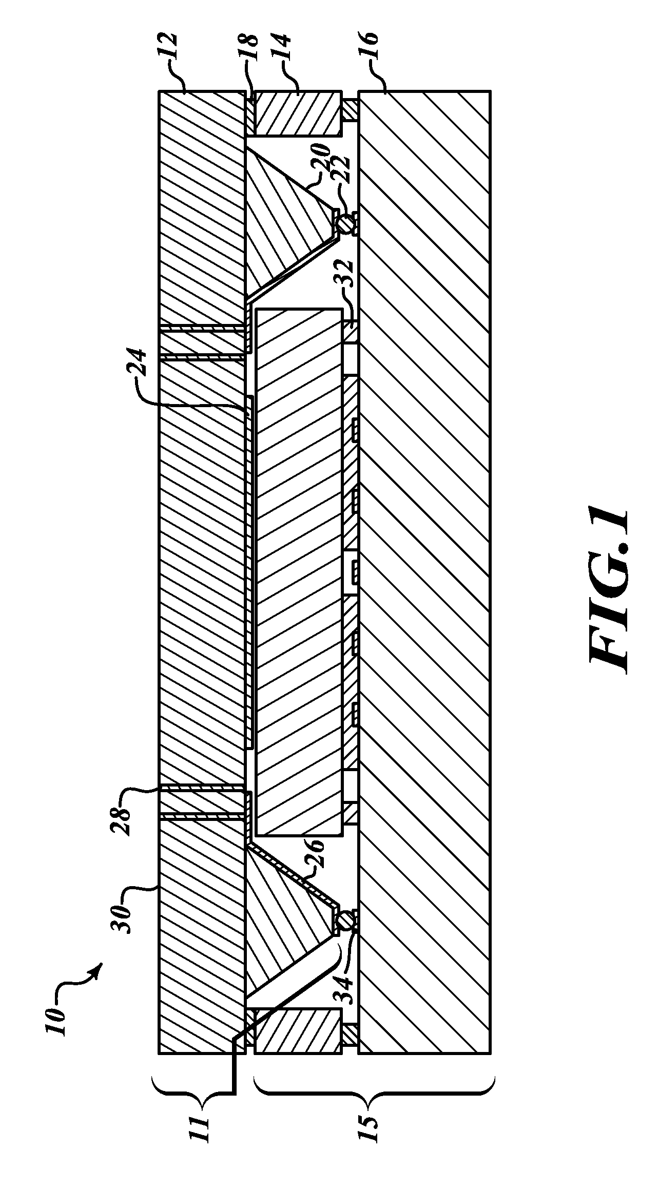
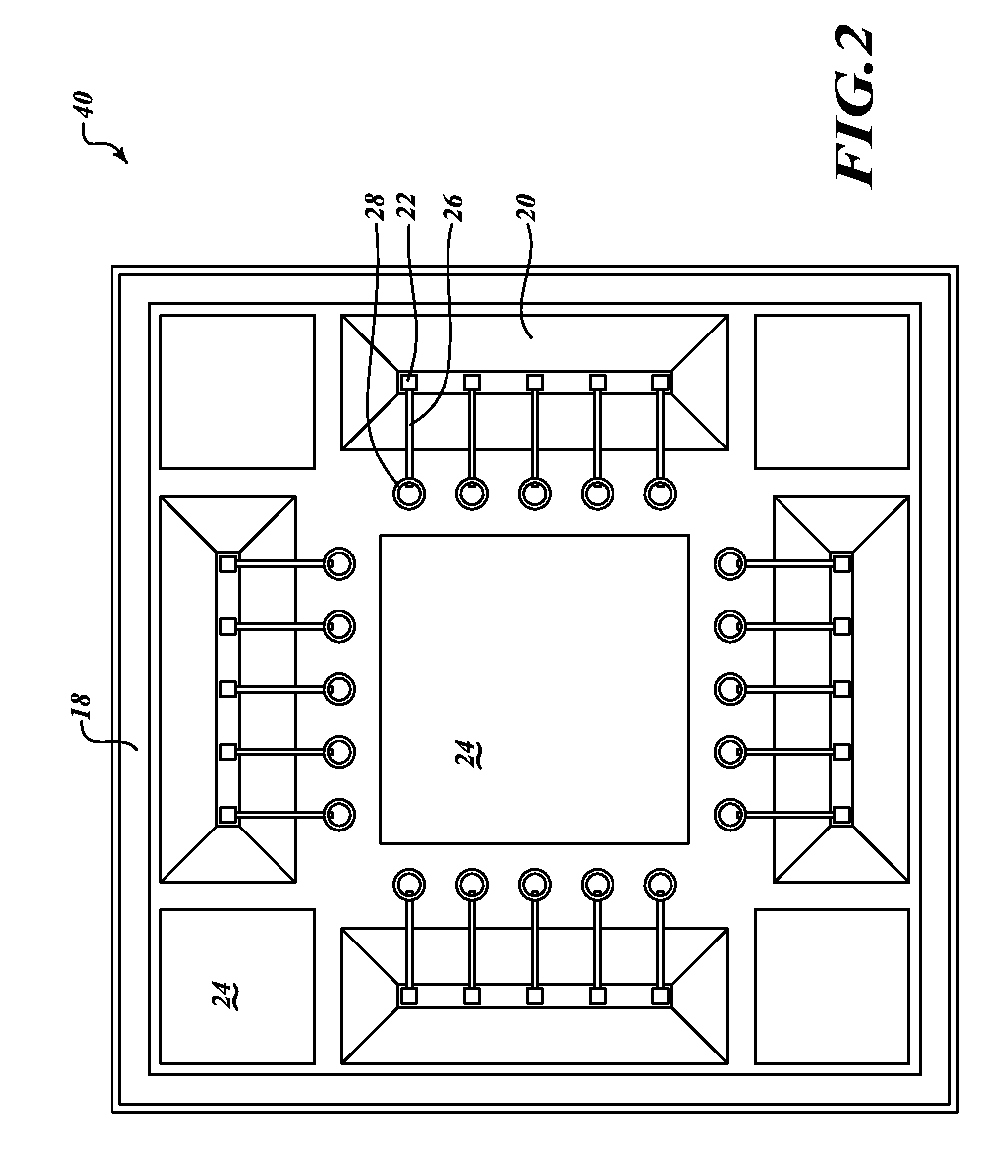
[0018]The present invention provides microelectromechanical sensor (MEMS) devices and fabrication processing methods for improving production yield by hermetically sealing a MEMS device with a hermetic interface chip (HIC) at the wafer level. Additionally, the MEMS devices and packaging techniques of the present invention eliminate almost all problems associated with presently available Wafer Level Packaging (WLP) techniques by hermetically sealing a MEMS device with an additional wafer, the HIC. FIG. 1 illustrates a side cross-sectional view of a hermetically sealed MEMS device 10 in accordance with an embodiment of the invention. The MEMS device 10 includes a HIC 11 having an upper substrate layer 12, feedthrough vias 28, an outer seal ring 18, and etched substrate mesas 20; and a device component 15 having an upper substrate layer 14, a mechanism device layer 32, and a lower substrate layer 16 with bond pads 34. The HIC 11 further includes internal 26 and external 30 conductive l...


PUM


Abstract

Systems and methods for enabling hermetic sealing at the wafer level during fabrication of a microelectromechanical sensor (MEMS) device. The MEMS device has a specialized hermetic interface chip (HIC) that facilitates a stable hermetic sealing process. The HIC includes a plurality of vias in a substrate layer, a plurality of mesas having etched portions, a seal ring, a plurality of conductive leads on a first side of the HIC, and a plurality of conductive leads on a second side of the HIC. The plurality of conductive leads on the first side of the HIC feeds from the etched portions of the plurality of mesas through the plurality of vias in the substrate layer to the plurality of conductive leads on the second side of the HIC. The conductive leads are capable of connecting an external circuit to the MEMS device.

Description

BACKGROUND OF THE INVENTION[0001]Many high performance MEMS devices, such as gyroscopes and accelerometers, are hermetically packaged in a vacuum or a gaseous environment. Hermetically sealing the substrate components within a MEMS device allows a vacuum or gas atmosphere to remain stable over time. Several MEMS device technologies today hermetically seal MEMS device substrates at the package level, after dicing of a sensing substrate wafer. This sealing typically occurs individually or in small batches during a separate fabrication processing step. A number of package level sealing (PLS) processes are utilized to hermetically seal MEMS devices, including: silicon to glass anodic bonding, silicon to silicon fusion bonding, and wafer to wafer bonding, utilizing various intermediate bonding agents.[0002]PLS can lead to problematic effects such as stiction between a sensing wafer and substrate components during a bonding process and lower production yield of MEMS devices. To eliminate ...

Claims


Application Information

Patent Timeline
IPC IPC(8): H01L23/02H01L21/50
CPCB81B7/0038B81B7/007
Inventor HORNING, ROBERT D.WILLITS, DAVID S.
Owner HONEYWELL INT INC
Why Eureka
Try Eureka