

Contact detecting device, display device, and contact detecting method
- Summary
- Abstract
- Description
- Claims
- Application Information
AI Technical Summary
Benefits of technology
Problems solved by technology
Method used
Image

Examples
first embodiment
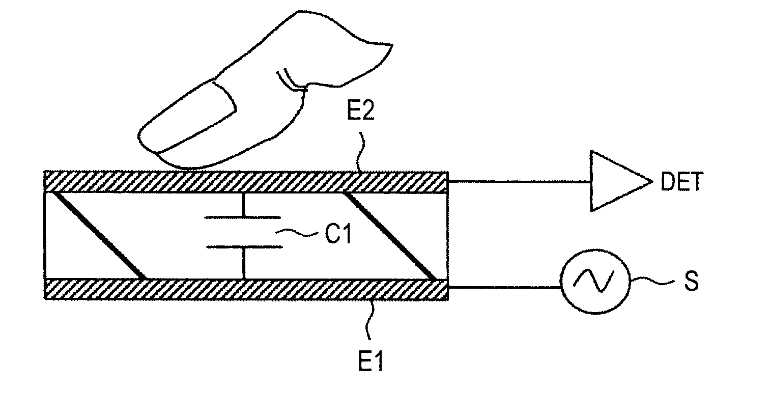
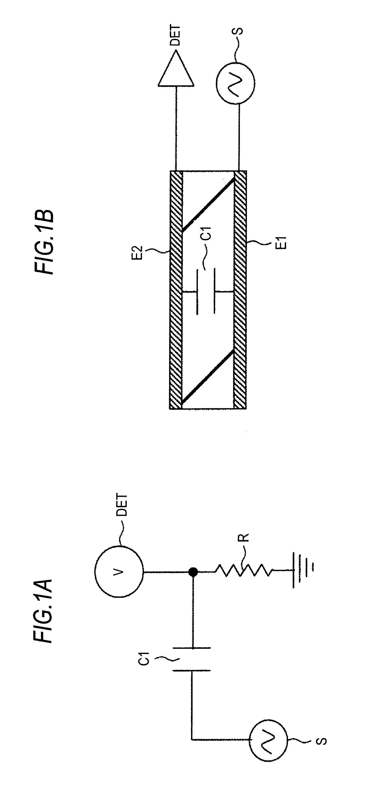
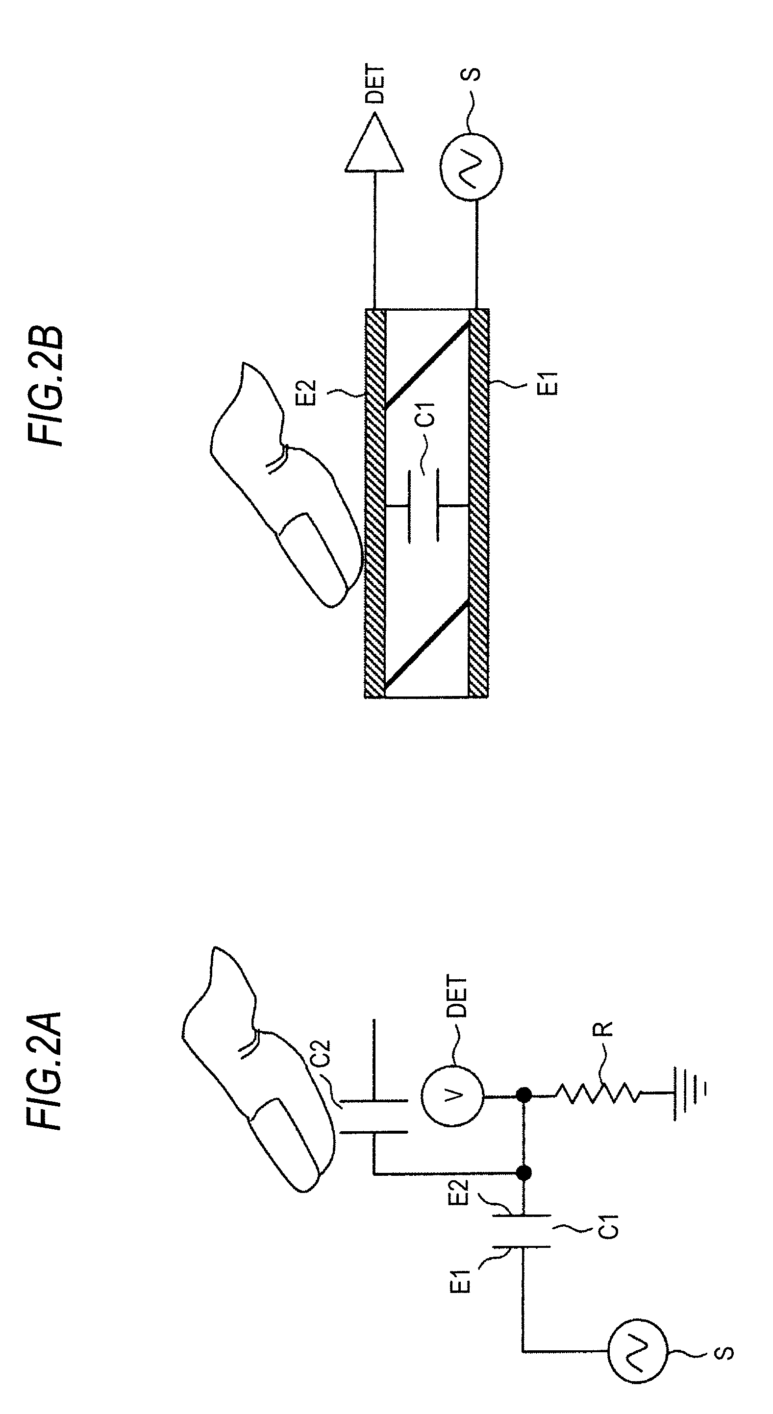
[0077]A contact detecting device according to a first embodiment of the present invention is explained below. As an example, the contact detecting device is a capacitance-type touch panel that can be externally attached to a display panel.
[0078]FIGS. 4A to 4C are plan views for specifically explaining electrodes of the contact detecting device according to this embodiment and circuits for driving and detection of the electrodes. FIG. 4D is a schematic sectional view of the sectional structure of the contact detecting device according to this embodiment externally attached to a display surface side of a liquid crystal display panel. In FIG. 4D, a section for six pixels in, for example, a row direction (a pixel display line direction) is shown.
[0079]In FIG. 4D, to facilitate understanding of the sectional structure, counter electrodes, pixel electrodes, and detection electrodes are hatched. However, concerning other sections (substrates, insulating films, functional films, etc.), the ...
second embodiment
[0181]In a second embodiment of the present invention, driving electrodes that are provided further in the inside of a panel than detection electrodes of a touch sensor (electrodes on a display surface side that a finger or the like approaches) and between which and the detection electrodes capacitors are formed are also used as electrodes for liquid crystal control. The electrodes are desirably provided to be opposed to both the detection electrodes and pixel electrodes. Therefore, the electrodes are hereinafter simply referred to as “counter electrodes”.
[0182]On the other hand, as the electrodes for liquid crystal control, a common electrode (so-called Vcom driving electrode) provided in common to plural pixels in order to apply an electric field to a display function layer such as a liquid crystal layer is provided to be opposed to the pixel electrodes for the respective pixels and used. In liquid crystal display control, a common driving signal Vcom given to the common electrode...
third embodiment
[0239]A third embodiment of the present invention is explained below. In this embodiment, unlike the second embodiment, a liquid crystal element of a horizontal field mode is used as a display element.
[0240]FIG. 16 is a schematic sectional diagram of a display device according to this embodiment. In FIG. 16, components same as those in the second embodiment are denoted by the same reference numerals and signs. Explanation of the components is omitted as appropriate.
[0241]The display device according to this embodiment is different from that according to the second embodiment in that the counter electrode 43 is arranged on the driving substrate 2 side. The counter electrode 43 in this embodiment is arranged to be opposed to the pixel electrodes 22 on an inverse liquid crystal layer side of the pixel electrodes 22. The opposed arrangement is not specifically shown in the figure. A distance between the pixel electrodes 22 is set relatively large. The counter electrode 43 causes an elec...
PUM
 Abstract
Description
Claims
Application Information