Solid-state imaging device and imaging device

a technology of imaging device and solid-state imaging, which is applied in the direction of instruments, television systems, color signal processing circuits, etc., to achieve the effect of enhancing the output of signal

Active Publication Date: 2010-04-15
PANASONIC SEMICON SOLUTIONS CO LTD
View PDF4 Cites 31 Cited by
  • Summary
  • Abstract
  • Description
  • Claims
  • Application Information

AI Technical Summary

Benefits of technology

[0033]The read-out unit reads out the difference during the analog to di

Problems solved by technology

Furthermore, by reducing longitudinal noises, it is unnecessary

Method used


Image

  • Solid-state imaging device and imaging device
  • Solid-state imaging device and imaging device
  • Solid-state imaging device and imaging device

Examples


embodiment 1

[0046]With reference to the drawings, a description is given of a solid-state imaging device pertaining to an embodiment of the present invention.

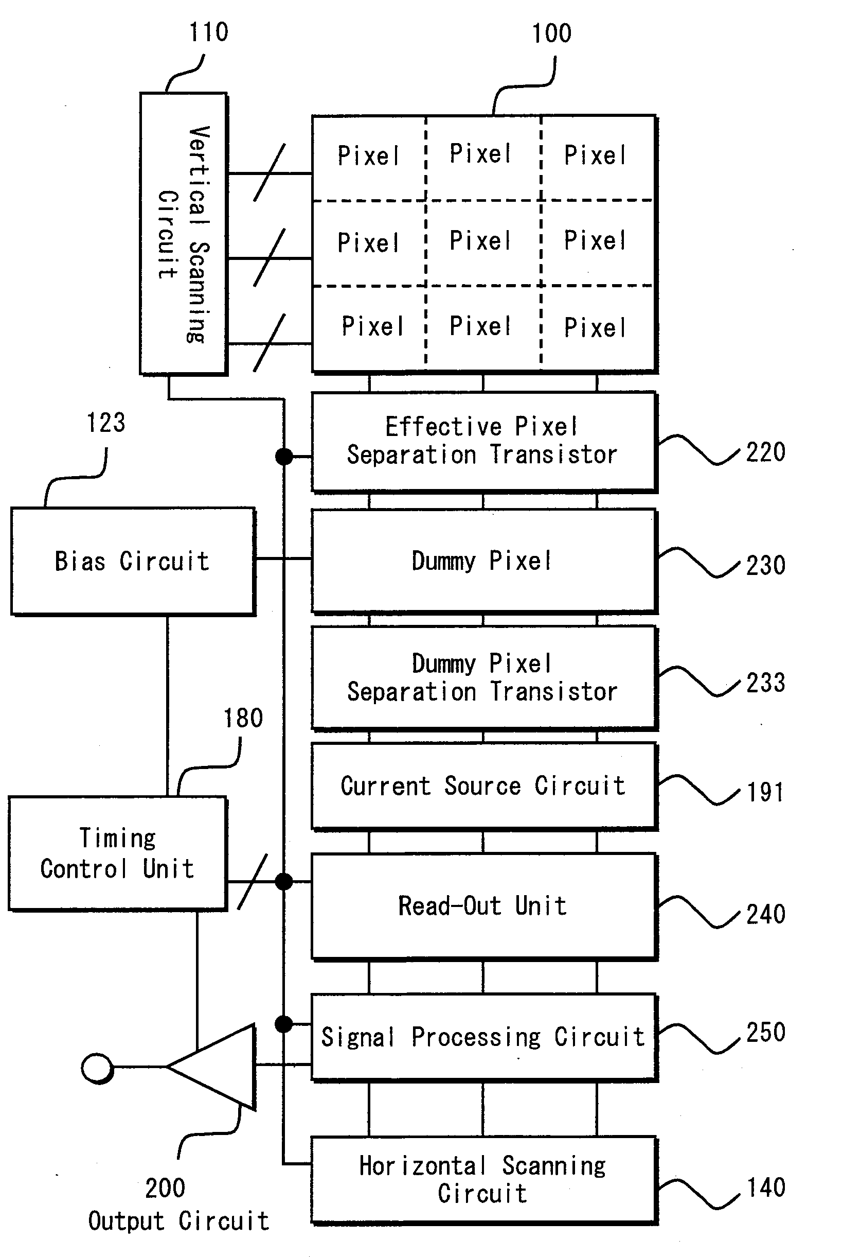
[0047]FIG. 4 is a schematic block diagram pertaining to Embodiment 1 of the present invention.

[0048]According to FIG. 4, the solid-state imaging device has a pixel area 100 where a plurality of pixels are arranged in a matrix, a vertical scanning circuit 110 that selects a pixel row, an effective pixel separation transistor 220, a dummy pixel 230, a dummy pixel separation transistor 233, a current source circuit 191, a read-out unit 240, a signal processing circuit 250, a horizontal scanning circuit 140, an output circuit 200 composed of an analog front end, an A / D convertor (ADC), an output processing unit or the like, a bias circuit 123 supplying a reference voltage to the dummy pixel, and a timing control unit 180. The effective pixel separation transistor 220, the dummy pixel 230, the dummy pixel separation transistor 233, the current ...

embodiment 2

[0121]Subsequently, a description is given of a solid-state imaging device pertaining to Embodiment 2 of the present invention. A description of the configuration of Embodiment 2 similar to that of Embodiment 1 is omitted.

[0122]FIG. 9 is a circuit configuration diagram showing the solid-state imaging device pertaining to Embodiment 2 of the present invention.

[0123]Differences between Embodiments 1 and 2 are the configurations of the effective pixel and the dummy pixel. According to Embodiment 1, the selection transistors 105 and 232 are provided. However, according to Embodiment 2, the selection transistors 105 and 232 are not provided. An effective pixel is selected by pulse-driving a pixel power supply.

[0124]According to Embodiment 1, the pixel dummy amplification transistors 231 may be provided in plural in one column with a size ratio of the width (W) and the length (L) of the path of the amplification transistor 103 in the effective pixel kept constant. Embodiment 2 is characte...


PUM


Abstract

Solid-state imaging device having a plurality of vertical signal lines, includes for each vertical signal line, an effective pixel and a dummy pixel, a switch transistor provided on a path connecting the dummy pixel and the vertical signal line, and a read-out unit. The switch transistor is OFF while a first signal is outputted from the effective pixel and ON while a second signal is outputted from the dummy pixel. The read-out unit (i) reads out a level of the first signal while the switch transistor is OFF, and (ii) reads out a difference between the level of the first signal and a level of the second signal when the switch transistor is turned from OFF to ON.

Description

[0001]This application is based on the disclosure of Japanese Patent Application No. 2008-263859 filed on Oct. 10, 2008, including specification, drawings, and claims is incorporated herein by reference in its entirety.BACKGROUND OF THE INVENTION[0002](1) Field of the Invention[0003]The present invention relates to a solid-state imaging device and an imaging device, particularly to a MOS type solid-state imaging device, such as a CMOS (Complementary Metal Oxide Semiconductor) image sensor.[0004](2) Description of the Related Art[0005]When extremely strong light, such as sunlight, is incident on a CMOS image sensor, an output signal thereof is radically lowered so that a portion corresponding to the lowered signal appears dark. Such a problem occurred in a CMOS image sensor is called a black-crush phenomenon. To suppress this phenomenon, the following method is proposed. An amplifier (amp) that does not have a photodiode (hereinafter, referred to as pixel dummy amplification transist...

Claims


Application Information

Patent Timeline
IPC IPC(8): H04N5/335H04N5/341H04N5/355H04N5/357H04N5/374H04N5/3745H04N5/378
CPCH04N5/378H04N5/3598H04N25/627H04N25/75
Inventor MURAKAMI, MASASHI
Owner PANASONIC SEMICON SOLUTIONS CO LTD
Why Eureka
Try Eureka