Solid-state image sensor and imaging apparatus equipped with solid-state image sensor

a technology of image sensor and image sensor, which is applied in the direction of radio frequency control devices, instruments, television systems, etc., can solve the problems of lower interpolation accuracy and image quality, lower interpolation accuracy, and lower image quality, so as to achieve lower interpolation accuracy and lower image quality

Active Publication Date: 2010-04-15
NIKON CORP
View PDF8 Cites 114 Cited by
  • Summary
  • Abstract
  • Description
  • Claims
  • Application Information

AI Technical Summary

Problems solved by technology

This means that since imaging pixels that output signals in a color matching that of the image signal to be generated in correspondence to the position assumed by a given focus detection pixel through the interpolation processing described earlier, are not present in close proximity to the focus detection pixel, the interpolation processing must be executed by using the output signals generated at imaging pixels located away from the focus detection pixel, which is bound to result in lower interpolation accuracy and lower image quality.
Since imaging pixels that output signals in a color matching that of the image signal to be generated in correspondence to the position assumed by each focus detection pixel through the interpolation processing described earlier are not present in close proximity to the focus detection pixel, the interpolation processing must be executed by using the output signals generated at imaging pixels located away from the focus detection pixel, which is bound to result in lower interpolation accuracy and lower image quality.

Method used


Image

  • Solid-state image sensor and imaging apparatus equipped with solid-state image sensor
  • Solid-state image sensor and imaging apparatus equipped with solid-state image sensor
  • Solid-state image sensor and imaging apparatus equipped with solid-state image sensor

Examples


first embodiment

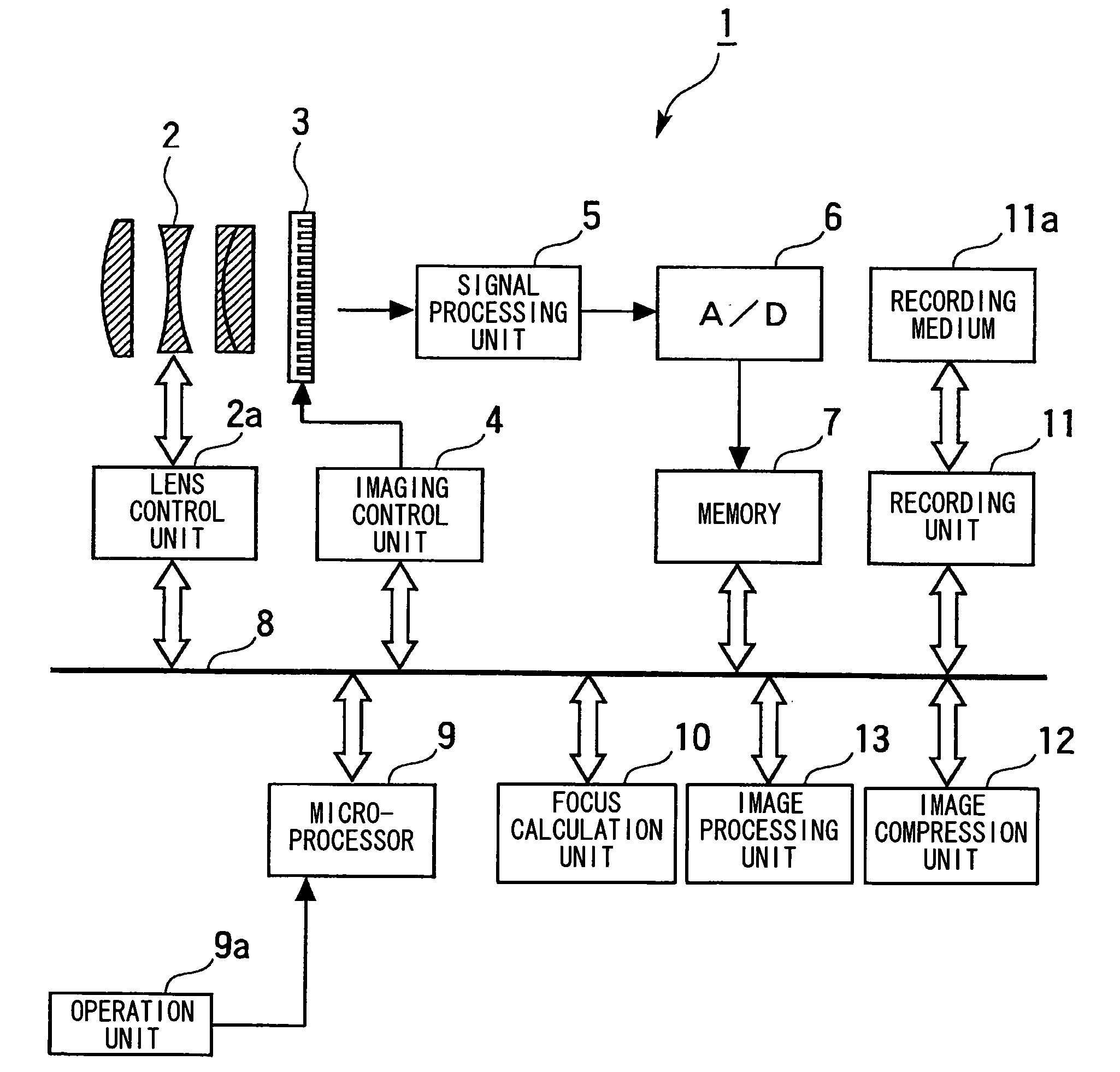
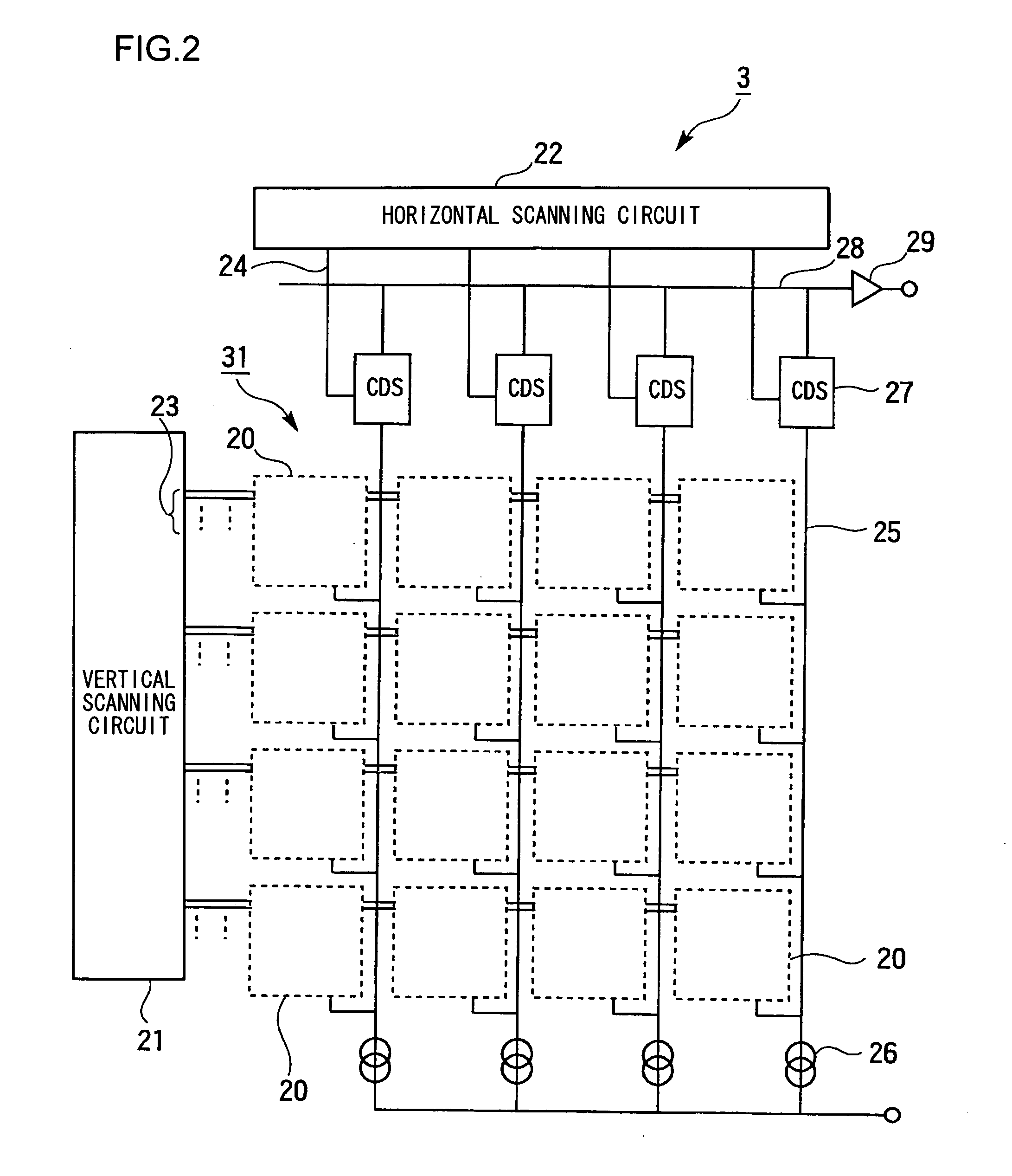
[0060]FIG. 1 is a schematic block diagram of an electronic camera 1 achieved in the first embodiment of the imaging apparatus according to the present invention. A photographic lens 2, used as an optical system through which a subject image is formed, is mounted at the electronic camera 1. As a lens control unit 2a drives the photographic lens 2, the focus and the aperture are adjusted. An imaging surface of a solid-state image sensor 3, which executes photoelectric conversion for the subject image formed via the photographic lens 2, is set within the image space of the photographic lens 2.

[0061]The solid-state image sensor 3 outputs signals as it is driven in response to a command issued by an imaging control unit 4. The solid-state image sensor 3 outputs imaging signals used to form image signals expressing a subject image and focus detection signals used to detect the focusing condition of the photographic lens 2. The imaging signals or the focus detection signals first undergo p...

second embodiment

[0110]FIG. 14, which corresponds to FIG. 4, is a schematic plan view showing in a partial enlargement the pixel arrangement adopted in a solid-state image sensor 90 in the electronic camera achieved in the second embodiment of the present invention. In FIG. 14, the same reference numerals are assigned to elements identical to or corresponding to those in FIG. 4 to preclude the necessity for a repeated explanation thereof.

[0111]The embodiment differs from the first embodiment in that the solid-state image sensor 90 is used in place of the solid-state image sensor 3. The following features of the solid-state image sensor 90 differentiate it from the solid-state image sensor 3. It is to be noted that while the focus detection areas 34˜37 are mentioned below, their illustration is not provided.

[0112]While the focus detection areas 32, 36 and 37 ranging along the X axis are each made up with pixels disposed in a single row and the pixel areas 33˜35 ranging along the Y axis are each made ...

third embodiment

[0115]FIG. 15, which corresponds to FIG. 3, is a schematic plan view of a solid-state image sensor 100 (more specifically its effective pixel area 101) in the electronic camera achieved in the third embodiment of the present invention. FIGS. 16 and 17, corresponding to FIG. 4, each present a schematic plan view showing in a partial enlargement, the pixel arrangement adopted in the solid-state image sensor 100. FIG. 16 shows part of a middle area 101a in the effective pixel area 101 at the solid-state image sensor 100 in FIG. 15, whereas FIG. 17 shows part of an upper area 101b or a lower area 101c of the effective pixel area 101. FIG. 18, which corresponds to FIG. 10, is a circuit diagram assumed in each pixel block made up with 2×2 pixels 20 at the solid-state image sensor 100. In FIGS. 15 through 18, the same reference numerals are assigned to elements identical to or corresponding to the elements in FIGS. 4 and 10 so as to preclude the necessity for a repeated explanation thereof...


PUM


Abstract

A solid-state image sensor executing photoelectric conversion for a subject image includes: a plurality of pixels disposed in a two-dimensional pattern and each equipped with a photoelectric conversion unit that generates and stores an electrical charge, wherein: the plurality of pixels are each one of a first pixel and a second pixel; the plurality of pixels are divided into a plurality of pixel blocks; the pixel blocks each include m×n pixels with m pixels and n pixels among the plurality of pixels set respectively along a columnar direction and along a row direction; at least one of the pixels in each pixel block is the first pixel; color filters assuming a single color are disposed at first pixels belonging to a common pixel block; and at least one pixel in at least one pixel block among the plurality of pixel blocks is the second pixel.

Description

[0001]This application is a continuation of International Application No. PCT / JP2008 / 060965 filed Jun. 16, 2008.INCORPORATION BY REFERENCE[0002]The disclosure of the following applications are herein incorporated by reference: Japanese Patent Application No. JP2007-159607 filed Jun. 16, 2007; International Application No. PCT / JP2008 / 060965 filed Jun. 16, 2008.BACKGROUND OF INVENTION[0003]1. Field of the Invention[0004]The present invention relates to a solid-state image sensor and an imaging apparatus equipped with the solid-state image sensor.[0005]2. Description of Related Art[0006]Today, imaging apparatuses such as video cameras and electronic still cameras are widely used by consumers. Such a camera typically includes a solid-state image sensor which may be, for instance, a CCD sensor or an amplifier-type sensor. The solid-state image sensor is constituted with a plurality of pixels, each equipped with a photoelectric conversion unit that generates a signal charge in corresponde...

Claims


Application Information

Patent Timeline
Patent Type & Authority Applications(United States)
IPC IPC(8): H04N5/335H01L27/146H04N5/232H04N5/238H04N5/369H04N5/374H04N9/07
CPCH01L27/14609H01L27/14621H01L27/14623H04N9/045H01L27/14643H04N5/3696H01L27/14627H04N25/702H04N23/843H04N25/134
Inventor SUZUKI, SATOSHI
Owner NIKON CORP
Why Eureka
Try Eureka