Laser annealing method and laser annealing apparatus

a laser annealing and laser annealing technology, which is applied in the direction of spraying apparatus, testing/measurement of semiconductor/solid-state devices, manufacturing tools, etc., can solve the problems of difficult optimal control of parameters and laser beam intensity

Inactive Publication Date: 2010-04-15
JAPAN DISPLAY WEST
View PDF7 Cites 32 Cited by
  • Summary
  • Abstract
  • Description
  • Claims
  • Application Information

AI Technical Summary

Benefits of technology

[0015]According to the present embodiments, the optimal and uniform crystal quantit

Problems solved by technology

However, with existing technique, it is difficult to optimally control the parameters such as an intensity of t

Method used


Image

  • Laser annealing method and laser annealing apparatus
  • Laser annealing method and laser annealing apparatus
  • Laser annealing method and laser annealing apparatus

Examples


Embodiment Construction

[0028]The preferred embodiments of the present invention will be described in detail hereinafter with reference to the accompanying drawings. Note that, the description will be given in the following order.

[0029]1. Laser annealing apparatus (apparatus construction, apparatus operation, and point of crystallization by laser annealing).

[0030]2. Laser annealing method.

[0031]3. Examples (example of control portion of laser annealing apparatus, and example of laser annealing method).

1. Laser Annealing Apparatus

Apparatus Construction

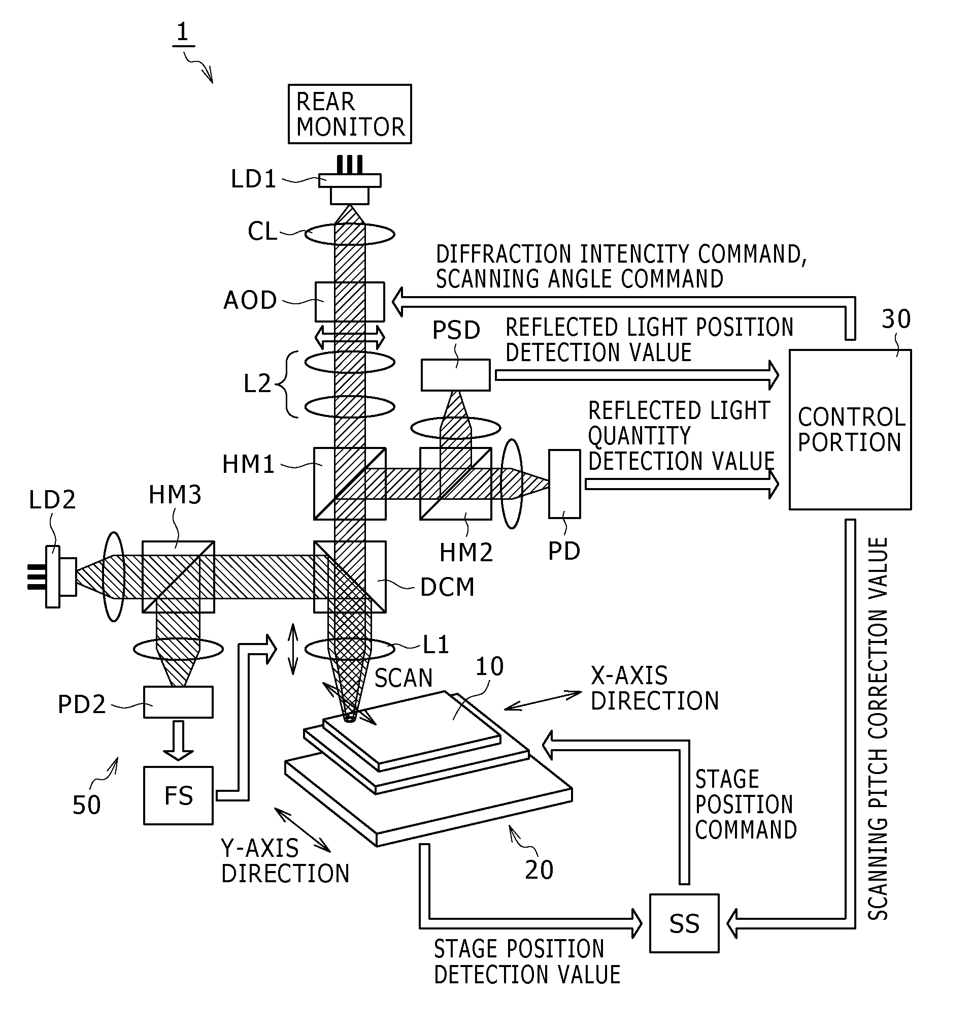
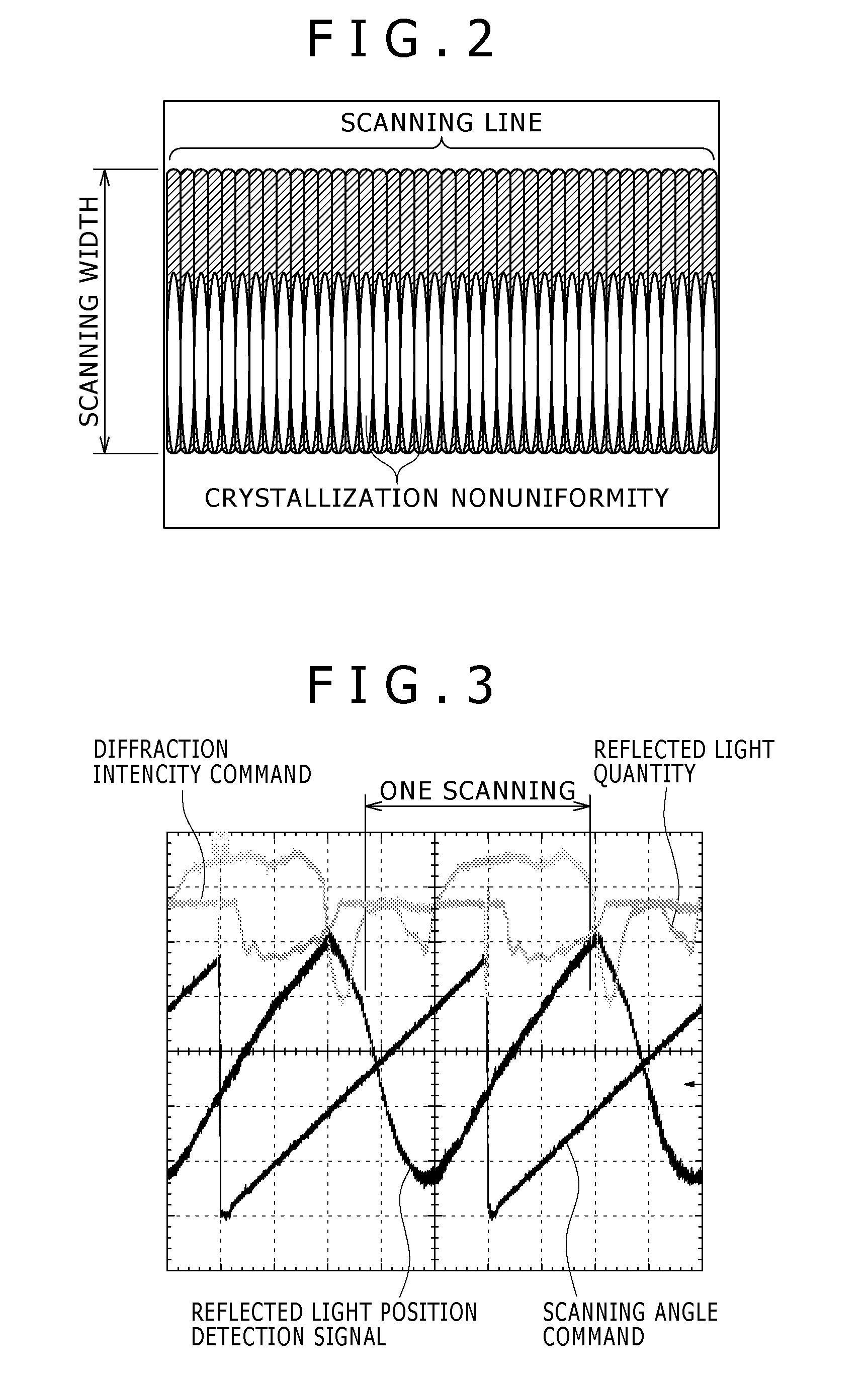
[0032]FIG. 1 is a schematic view showing a construction of a laser annealing apparatus according to an embodiment of the present invention. The laser annealing apparatus 1 of the embodiment is an apparatus for radiating a laser beam to an amorphous film on a substrate 10 while scanning the laser beam for the amorphous film on the substrate 10, thereby crystallizing the amorphous film. The feature of the laser annealing apparatus 1 of the embodiment is that in ...


PUM

PropertyMeasurementUnit
Speedaaaaaaaaaa
Lightaaaaaaaaaa

Abstract

An embodiment of the invention provides a laser annealing method, including the steps of radiating a laser beam to an amorphous film on a substrate while scanning the laser beam for the amorphous film, crystallizing the amorphous film, detecting a light quantity of laser beam reflected from the substrate and a scanning speed of the laser beam while the radiation and the scanning of the laser beam are carried out for the amorphous film, and controlling a radiation level and the scanning speed of the laser beam based on results of comparison of the light quantity of laser beam reflected from the substrate, and the scanning speed of the laser beam with respective preset references.

Description

BACKGROUND OF THE INVENTION[0001]1. Field of the Invention[0002]The present invention relates to a laser annealing method and a laser annealing apparatus, and more particularly to a laser annealing method and a laser annealing apparatus for radiating a laser beam to an amorphous film on a substrate while scanning the laser beam for the amorphous film, thereby crystallizing the amorphous film.[0003]2. Description of the Related Art[0004]In a flat type display device such as a liquid crystal display device or an organic Electro Luminescence (EL) display device, a Thin Film Transistor (TFT) is used as a switching element used to carry out active matrix display by using a plurality of pixels.[0005]A poly-Si TFT in which poly-Si, μc-Si or the like is used in an active region, and an amorphous Si TFT in which an amorphous Si is used in an active region are known as the TFT. Of these poly-Si TFT and the amorphous Si TFT, the poly-Si TFT has the feature that a mobility of a carrier is about...

Claims


Application Information

Patent Timeline
IPC IPC(8): H01L21/66B23K26/00H01L21/268
CPCH01L22/26B23K26/03
Inventor TAKAGI, KATSUJIMACHIDA, AKIOFUJINO, TOSHIOKONO, TADAHIROFUKASAWA, NORIOHAGA, SHINSUKE
Owner JAPAN DISPLAY WEST
Why Eureka
Try Eureka