Organic electroluminescent device, method for producing organic electroluminescent device, and electronic apparatus

a technology of electroluminescent devices and electroluminescent devices, which is applied in the manufacture of electrode systems, electric discharge tubes/lamps, instruments, etc., can solve the problems of uneven film thickness after drying, and achieve the effect of reducing thickness variations, improving design flexibility of hold capacitors corresponding to at least three organic el elements, and high surface flatness

Inactive Publication Date: 2010-04-22
SEIKO EPSON CORP
View PDF11 Cites 47 Cited by
  • Summary
  • Abstract
  • Description
  • Claims
  • Application Information

AI Technical Summary

Benefits of technology

[0011]The base layer, including the drive circuit sections of the organic EL elements, tends to have surface irregularities. In the above structure, however, the partitioning portion defines the first film-formation region such that at least parts of the drive circuit sections of at least two organic EL elements are disposed in the first film-formation region. This allows the base layer to have less surface irregularities in the second film-formation region than in the first film-formation region. Thus, the first and second film-formation regions have different levels (states) of surface irregularities. In the formation of the second organic EL element in the second film-formation region, therefore, at least a light-emitting layer is less affected by surface irregularities, so that it can be formed with reduced variations in thickness. Accordingly, at least the second organic EL element of the organic EL device can emit light with stable luminance.
[0042]In this case, the first light-emitting layer is formed in the first film-formation region by evaporation or spin coating because they provide superior coverage. The second light-emitting layer, on the other hand, is formed in the second film-formation region, where the base layer has a higher flatness than in the first film-formation region, by droplet ejection. Accordingly, the first and second light-emitting layers have reduced variations in thickness.

Problems solved by technology

In particular, if the organic functional layers are formed by droplet ejection (ink-jet process), the ejected liquid compositions tend to flow into a step region at the lowest level and may therefore lead to uneven film thickness after drying.

Method used


Image

  • Organic electroluminescent device, method for producing organic electroluminescent device, and electronic apparatus
  • Organic electroluminescent device, method for producing organic electroluminescent device, and electronic apparatus
  • Organic electroluminescent device, method for producing organic electroluminescent device, and electronic apparatus

Examples


first embodiment

Organic EL Device

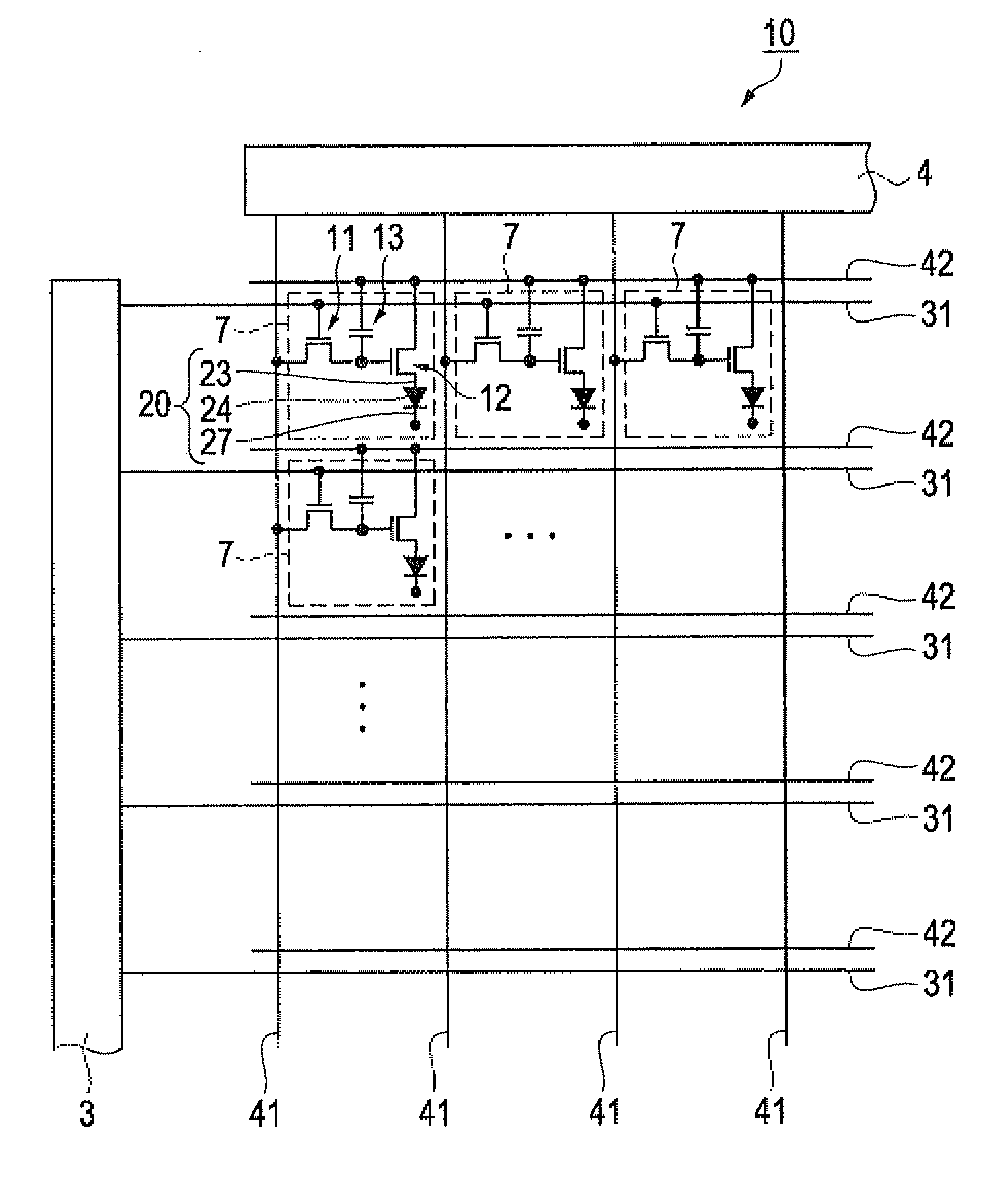
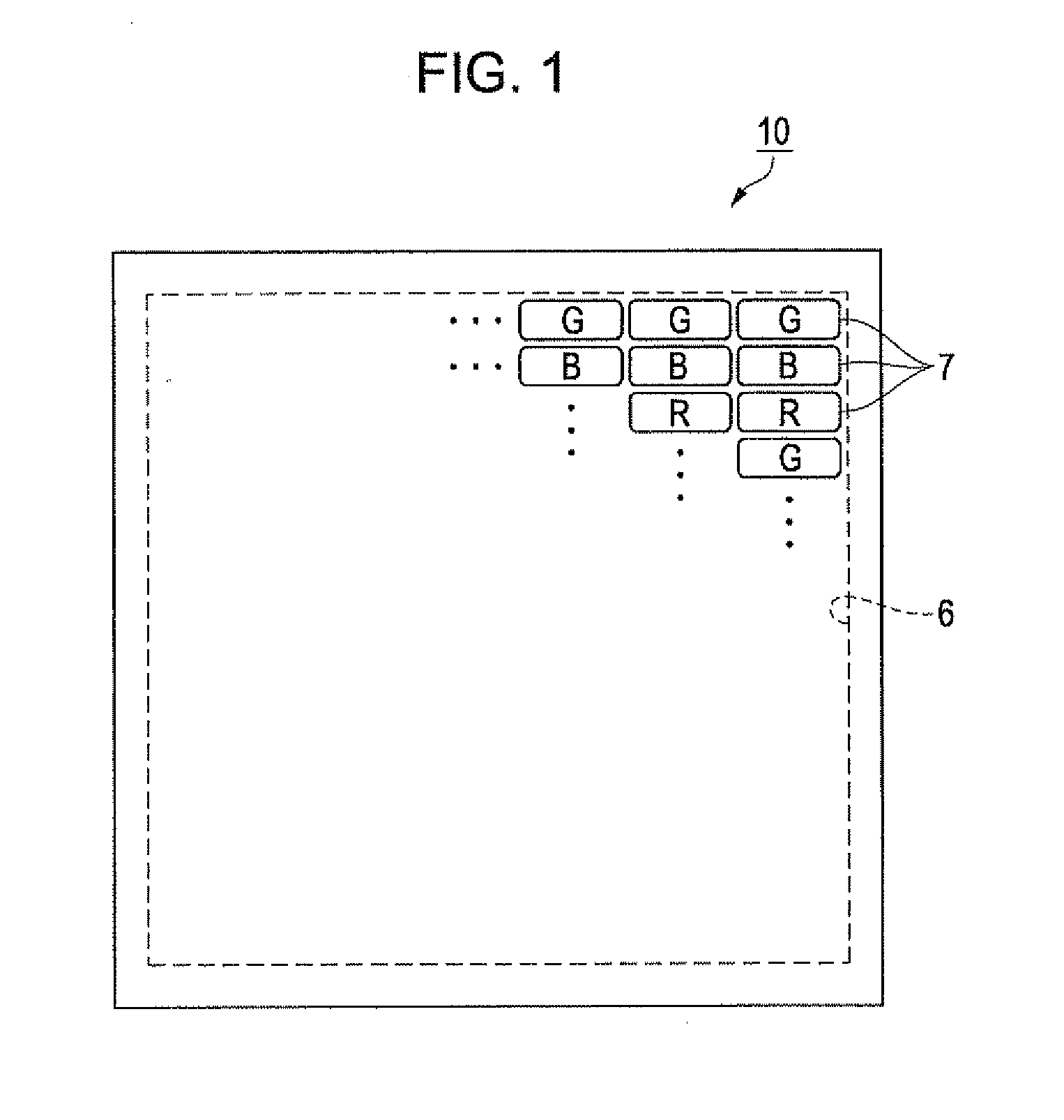
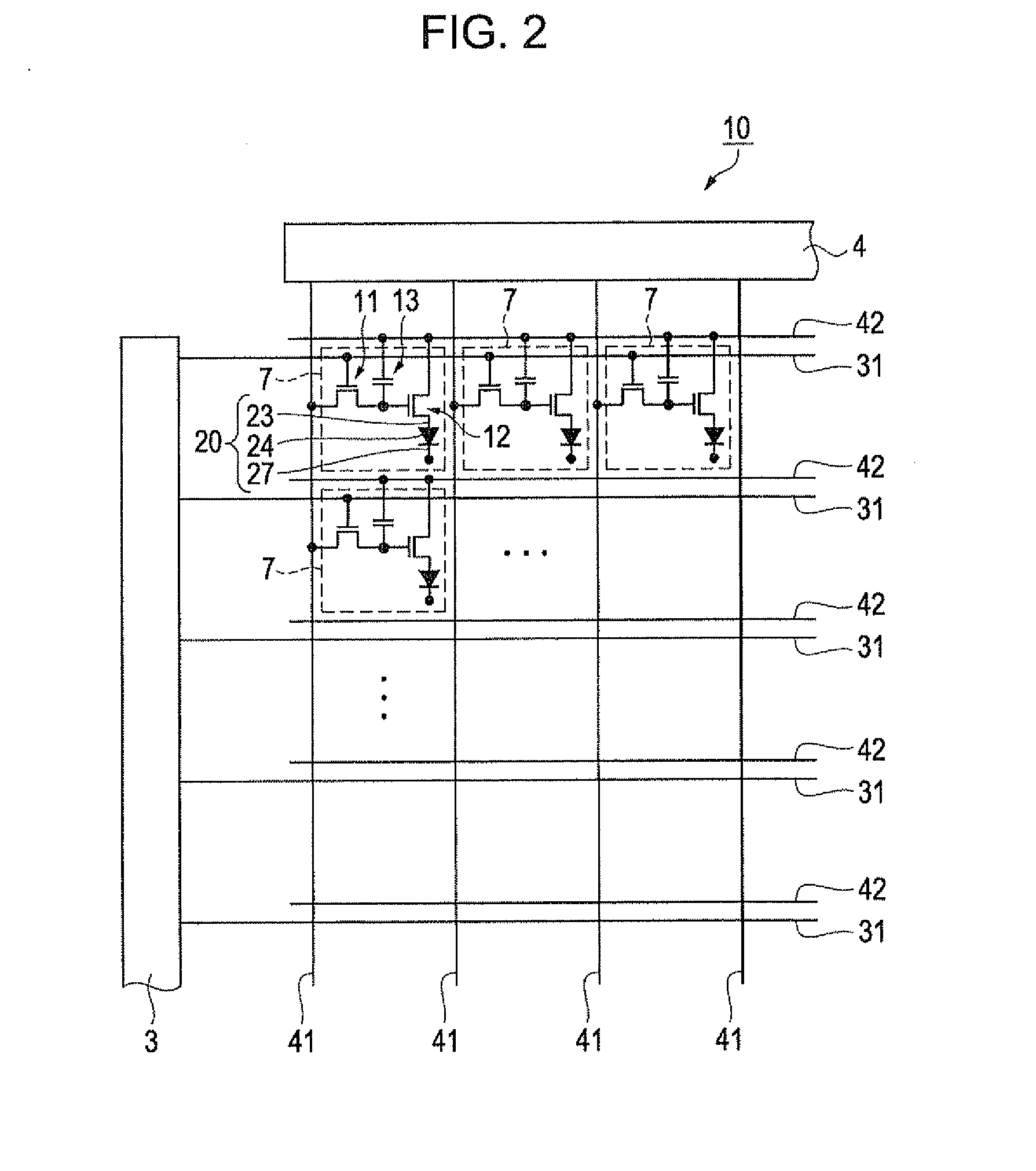
[0075]First, an organic EL device according to this embodiment will be described with reference to FIGS. 1 to 7. FIG. 1 is a schematic plan view of the organic EL device. FIG. 2 is an equivalent circuit diagram of the organic EL device. FIG. 3 is a schematic plan view showing the structure of light-emitting pixels. FIG. 4 is a plan view showing the detailed structure of the light-emitting pixels. FIG. 5 is a sectional view taken along line V-V of FIG. 4, showing the structure of the light-emitting pixels. FIG. 6 is a plan view showing the structure of light-emitting pixels in an organic EL device serving as a comparative example. FIG. 7 is a sectional view taken along line VII-VII of FIG. 6, showing the structure of the light-emitting pixels in the comparative example.

[0076]Referring to FIG. 1, an organic EL device 10 according to this embodiment has light-emitting pixels 7 that emit red (R), green (G), and blue (B) light (emission colors). The light-emitting pixels...

second embodiment

[0146]Next, an organic EL device according to a second embodiment of the invention will be described with reference to FIG. 11. FIG. 11 is a schematic diagram showing the pixel structure of the organic EL device according to the second embodiment. The same portions as those of the organic EL device 10 according to the first embodiment are denoted by the same reference numerals.

[0147]Referring to FIG. 11, an organic EL device 40 according to this embodiment includes scan lines 31 and data lines 41 arranged in a grid pattern and insulated from each other and power lines 42 disposed along the individual scan lines 31. The organic EL device 40 has emission control units Lu in regions defined by the scan lines 31 and the data lines 41. That is, the structure and arrangement of the emission control units Lu are the same as those of the organic EL device 10.

[0148]Depending on steps (level or state of surface irregularities) over the drive circuit sections formed on the substrate, each regi...

third embodiment

[0155]Next, organic EL devices serving as first to fourth examples of a third embodiment of the invention and methods for producing the organic EL devices will be described. The same portions as those of the organic EL device 10 according to the first embodiment are denoted by the same reference numerals.


PUM


Abstract

An organic EL device includes a base layer including a substrate, a partitioning portion disposed on the base layer and defining first and second film-formation regions adjacent to each other, a first organic EL element disposed on the base layer at a position overlapping the first film-formation region in plan view, a second organic EL element disposed on the base layer at a position overlapping the second film-formation region in plan view, a first drive circuit section disposed in the base layer to control driving of the first organic EL element, and a second drive circuit section disposed in the base layer to control driving of the second organic EL element. At least part of the first drive circuit section and at least part of the second drive circuit section overlap the first film-formation region in plan view.

Description

BACKGROUND[0001]1. Technical Field[0002]The present invention relates to organic electroluminescent (EL) devices having light-emitting elements, methods for producing organic EL devices, and electronic apparatuses.[0003]2. Related Art[0004]A known organic EL device disclosed in JP-A-2007-103032 has functional layers including light-emitting layers in substantially rectangular aperture regions separated by partitions. The aperture regions have narrow portions formed by reducing the width between the long sides thereof at the center of the long sides in the lengthwise direction.[0005]Another known organic EL device disclosed in JP-A-2007-227127 includes first partitions separating pixels of different colors and second partitions partially separating pixels of the same colors. Organic functional layers formed in adjacent pixels of the same colors are connected via regions where no second partitions are formed.[0006]In the light-emitting devices disclosed in the above publications, the ...

Claims


Application Information

Patent Timeline
Patent Type & Authority Applications(United States)
IPC IPC(8): H01K1/62H01J9/00
CPCH01L27/3211H01L27/3276H01L27/326H01L27/3246H10K59/352H10K59/353H10K59/121H10K59/122H10K59/131H10K50/813G09G3/3233H10K59/35
Inventor KITABAYASHI, ATSUSHIGOTO, MASASHIMISAWA, RYUHEI
Owner SEIKO EPSON CORP
Why Eureka
Try Eureka