Susceptor for epitaxial growing and method for epitaxial growing

A technology of epitaxial growth and susceptor, applied in chemical instruments and methods, crystal growth, single crystal growth, etc., can solve problems such as wafer quality deterioration, achieve quality and yield improvement, and achieve the effect of uniform epitaxial layer thickness

Inactive Publication Date: 2015-07-01
LG SILTRON
View PDF5 Cites 13 Cited by
  • Summary
  • Abstract
  • Description
  • Claims
  • Application Information

AI Technical Summary

Problems solved by technology

As the thickness deviation becomes more severe, the quality of the wafer deteriorates more severely, and more problems arise in forming semiconductor devices

Method used


Image

  • Susceptor for epitaxial growing and method for epitaxial growing
  • Susceptor for epitaxial growing and method for epitaxial growing
  • Susceptor for epitaxial growing and method for epitaxial growing

Examples


Embodiment approach

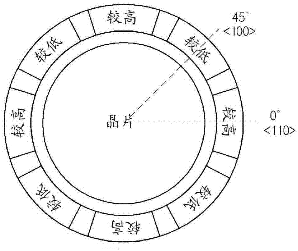
[0060] Described below is an embodiment in which a higher region on which the first gas regulating member is formed and a lower region on which the second gas regulating member is formed are asymmetrically formed with respect to the buffer region.

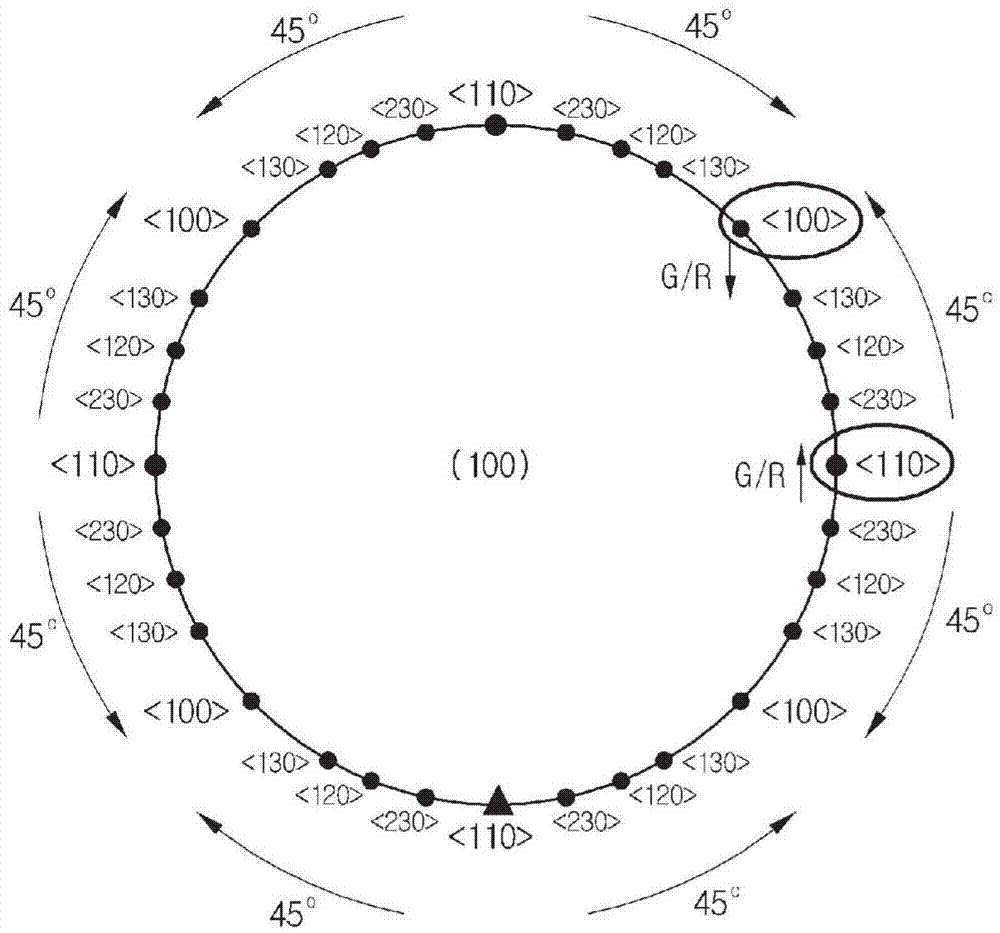
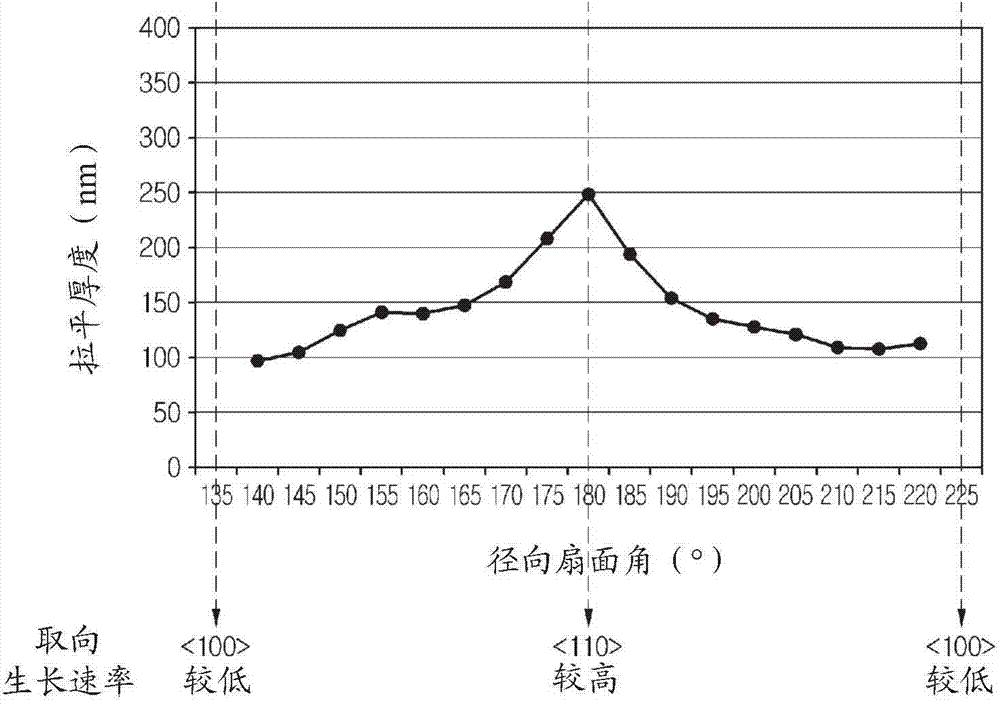
[0061] Figure 9 is a schematic diagram showing the region where the gas regulating member is formed on the susceptor according to Comparative Example 2, and Figure 10 is a simplified diagram showing a region where a gas regulating member is formed on a susceptor according to an embodiment. will refer to Figure 9 and Figure 10 Embodiments are described.

[0062] Figure 9 The thicknesses of certain regions of the wafer on the Comparative Example 2 susceptor are shown, more specifically, regions corresponding to angles between about 135 degrees and about 225 degrees as shown in FIG. 8 . From Figure 9 It can be understood that the thickness of the edge portion of the wafer is greatest at the center of the higher region of t...


PUM


Abstract

The present invention relates to a susceptor for manufacturing an epitaxial wafer in which an epitaxial layer is grown through a reaction between a wafer and a source gas in a chamber, including a pocket where an opening portion is formed for the wafer to be arranged; a ledge portion where the wafer is supported; and a gas adjusting member that is positioned in an outer circumferential portion on an upper surface of the opening portion of the susceptor. The gas adjusting member has a first gas adjusting member that is formed in a predetermined area which faces a crystallization direction of the wafer <110>; a second gas adjusting member in a predetermined area that faces the crystallization direction of the wafer <110>; and a third gas adjusting member that is formed between the first gas adjusting member and the second gas adjusting member. The first gas adjusting member, the second gas adjusting member, and the third gas adjusting member are formed to have different sizes in the areas which are formed along the circumference of the wafer, and the first, second, and third gas adjusting members are formed to have different degrees of inclination from the central direction of the wafer toward the susceptor so as to change the gas flow. Accordingly, the different areas where the gas flow increasing and decreasing devices (gas adjusting members) are formed are formed in the outer circumferential portion of the susceptor, and thus a deviation in the thickness of the epi layer in a wafer edge portion can be decreased when the epitaxial layer is formed in the semiconductor wafer.

Description

technical field [0001] The present invention relates to a susceptor for manufacturing epitaxial wafers, and more particularly to a susceptor for controlling the flatness of an edge portion of a wafer. Background technique [0002] Silicon epitaxial wafers are produced by vapor-phase-growing silicon epitaxial layers on silicon wafers doped with impurities such as boron (B) to have low resistivity, and the silicon epitaxial layers are doped with less impurities to have a high resistivity. The silicon epitaxial wafer has high collection capability at high temperature, low latch-up characteristics and anti-slip characteristics, and thus is widely used in the manufacture of MOS devices and LSI devices. [0003] The quality evaluation items for such epitaxial wafers may include: flatness and degree of particle contamination for evaluating the surface of the epitaxial wafer including the substrate and the epitaxial layer; and epitaxial layer thickness uniformity, resistivity and i...

Claims


Application Information

Patent Timeline
Patent Type & Authority Applications(China)
IPC IPC(8): H01L21/683H01L21/205C23C16/44
CPCC23C16/45591C23C16/4585C30B25/12C30B25/165H01L21/68735C23C16/458C30B29/06H01L21/68785
Inventor 姜侑振
Owner LG SILTRON
Why Eureka
Try Eureka