

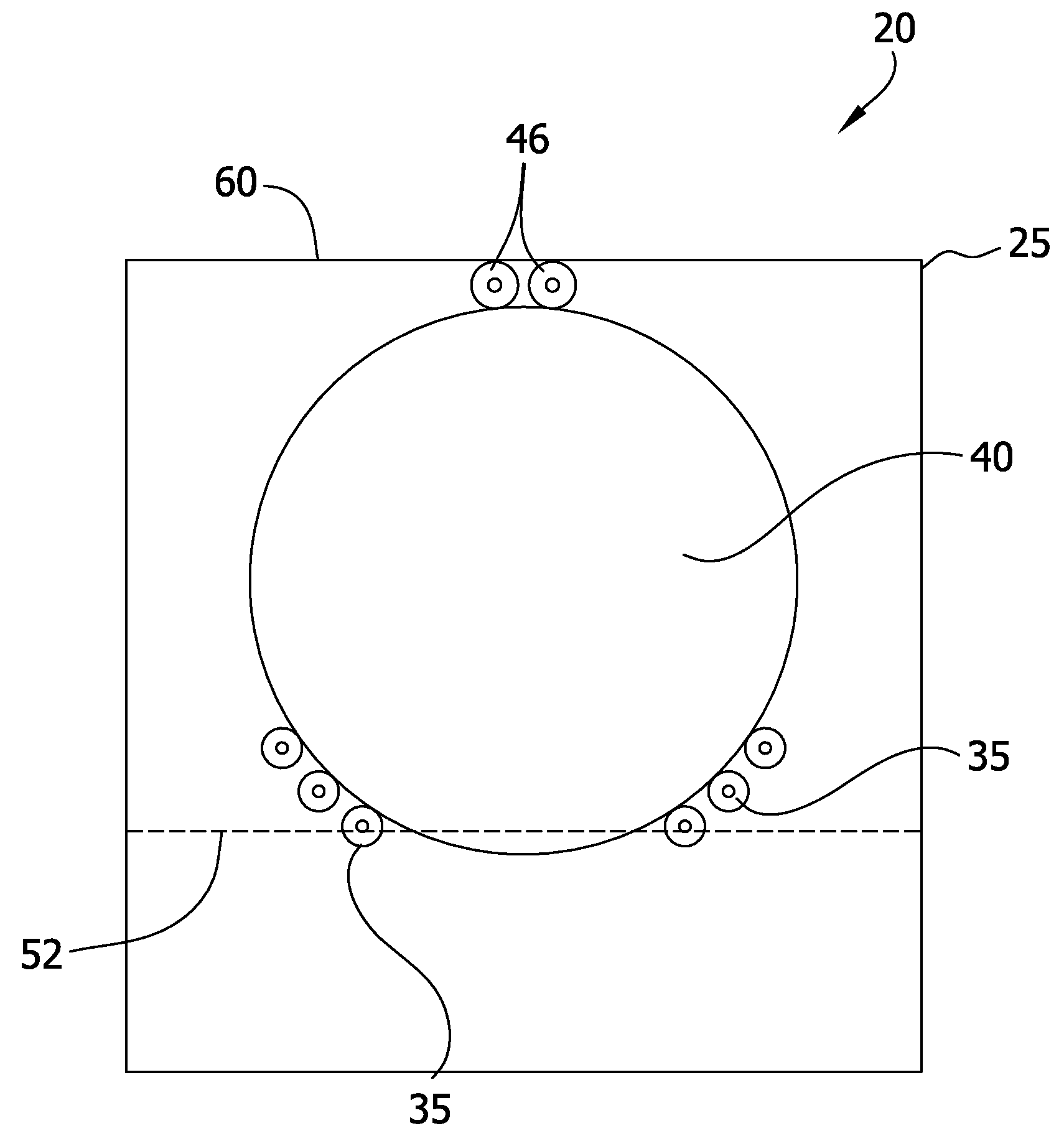
Edge etching apparatus for etching the edge of a silicon wafer
a silicon wafer and edge etching technology, which is applied in electrical apparatus, thin material processing, transportation and packaging, etc., can solve the problems of edge slippage, surface defects, and residual film deposits at the edge that may flake off, and achieve the effect of reducing the total thickness variation of the edge etching wafer
- Summary
- Abstract
- Description
- Claims
- Application Information
AI Technical Summary
Benefits of technology
Problems solved by technology
Method used
Image

Examples
example 1
Evaluation of Edge Quality of Edge Etched Wafers
[0091]Edge portions of 15 P− 300 mm wafers were etched utilizing an edge etcher of the type shown in FIGS. 6-9. The edge portions were immersed in a pool of 300 ml of acidic etchant from the following mixture: 2.4 l of HNO3 (69 wt. %), 2 l of H3PO4 (85 wt %) and 0.55 l of HF (49 wt %).
[0092]Two runs were carried out, one in which an edge portion of 7 wafers were etched with the edge portion extended from the nearest peripheral edge point to a point approximately 8.5 mm from the nearest peripheral edge point. In the second run 8 wafers were etched with the edge portion extending to a point approximately 8.5 mm from the nearest peripheral edge point.
[0093]The etch time of the first, 7 wafer run was 300 seconds, with rotation reversal after 150 seconds. Silicon removal, based on OGP diameter (a comparison of wafer diameter prior to and after etching) was approximately 30 μm.
[0094]The etch time of the second, 8 wafer run was 360 seconds, w...
example 2
Determination of the Amount of Material Removed by Edge Etching
[0098]300 mm wafers (75) were cut from a single crystal silicon ingot. After edge grinding, the edge portions of the wafers were etched utilizing an edge etcher of the type shown in FIGS. 6-9.
[0099]The wafers were split into a first group of 39 wafers and a second group of 36 wafers. The first group of wafers was edge polished (EP-300-X, SpeedFam) for 11 seconds and the second group was edge polished for 8 seconds.
[0100]A third group (75) of wafers was cut from a single wafer and subjected to edge grinding and edge polishing (EP-300-X, SpeedFam). The edge polish was a conventional 13 seconds in length.
[0101]The edge etched wafers were then combined and double-sided polished. The wafers of the third group were also double-sided polished (AC-2000-P2, PeterWolters). The cassettes of all batches of wafers were combined and a finish polish was performed (LapMaster). The double-sided polish removed approximately 15 μm of mater...
example 3
Flatness Comparison between Wafers that were and were not Edge Polished
[0103]The flatness of the three batches of wafers of Example 2 was determined by both GBIR, SBIR and SFQR methods after finish polishing. The results are shown in Table 1 below.
TABLE 1Flatness data for edge etched wafers and non-edge etchedwafers after double-sided polishing and finish polishingAverageAverageAverage SBIR MaxSFQR MaxNon-Edge Etched (13 sec)308.7118.729.8Edge Etched (11 sec)315.9124.541.3Edge Etched (8 sec)299.8108.537.0
As can be seen from Table 1, edge etching did not significantly degrade the flatness of finish polished wafers.
PUM
| Property | Measurement | Unit |
|---|---|---|
| width | aaaaa | aaaaa |
| width | aaaaa | aaaaa |
| width | aaaaa | aaaaa |
Abstract
Description
Claims
Application Information