Method of forming an electrical contact in a semiconductor device using an improved self-aligned contact (SAC) process

a technology of self-aligning contact and semiconductor device, which is applied in the direction of semiconductor/solid-state device manufacturing, electrical equipment, basic electric elements, etc., can solve the problems of unwanted loss of portions of gate line and bit line and achieve the effect of reducing the thickness deviation of hard mask nitride layers

Active Publication Date: 2007-11-29
SK HYNIX INC
View PDF5 Cites 13 Cited by
  • Summary
  • Abstract
  • Description
  • Claims
  • Application Information

AI Technical Summary

Benefits of technology

[0025]Accordingly, the present invention has been made in an effort to solve or at least minimize some of the problems that are encountered in the related art, and an aspect of the present invention is to provide a method for forming a contact of a semiconductor device which can decrease the thickness deviation of a hard mask nitride layer when forming a contact.
[0026]Another aspect of the present invention is to provide a method for forming a contact of a semiconductor device which can decrease the polishing thickness of a conductive layer for a plug by decreasing the thickness deviation of a hard mask nitride layer.
[0027]Still another aspect of the present invention is to provide a method for forming a contact of a semiconductor device which can improve uniformity of a wafer by decreasing the polishing thickness of a conductive layer for a plug.

Problems solved by technology

One particular problem with conventional methods may occur when forming the landing plug contacts 12a and the storage node contacts 21a is that there results in the unwanted loss of portions of the gate line and the bit line hard mask nitride layers (4 and 16, respectively) when the first and second interlayer insulation layers (8 and 19, respectively) are differentially etched away.

Method used


Image

  • Method of forming an electrical contact in a semiconductor device using an improved self-aligned contact (SAC) process
  • Method of forming an electrical contact in a semiconductor device using an improved self-aligned contact (SAC) process
  • Method of forming an electrical contact in a semiconductor device using an improved self-aligned contact (SAC) process

Examples


Embodiment Construction

[0067]Reference will now be made in greater detail to preferred embodiments of the invention, examples of which are illustrated in the accompanying drawings.

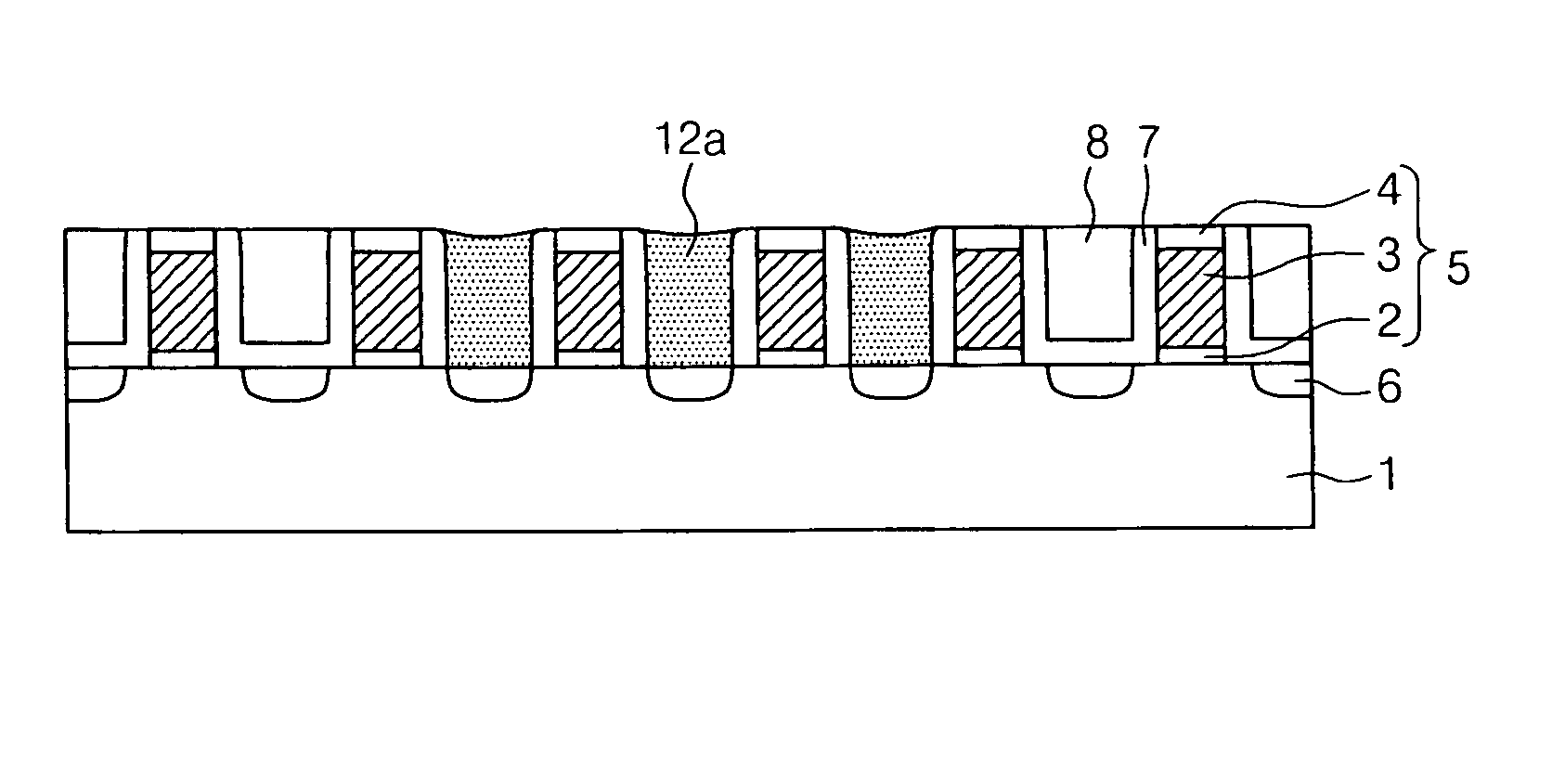
[0068]First describing the technical principle of the present invention, the present invention can be characterized by the fact that, when forming a landing plug contact 12a and a storage node contact 21a, a polysilicon hard mask pattern is only formed on an interlayer insulation layer such that entire gate lines and bit lines are opened.

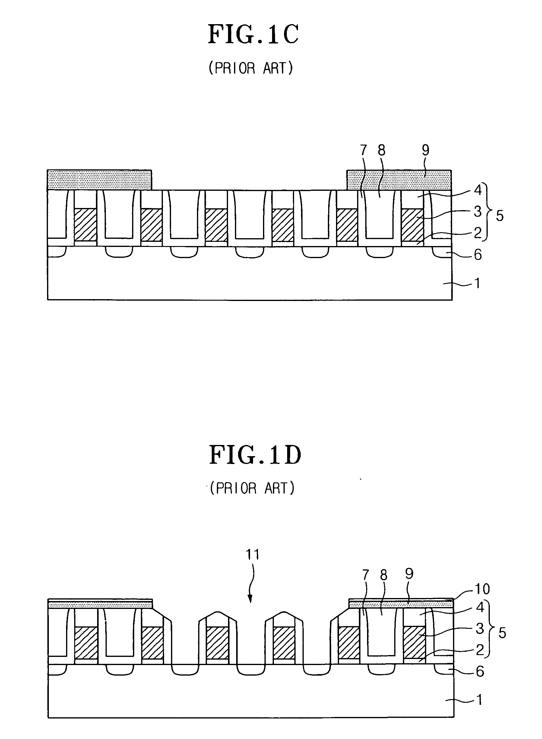
[0069]In this case, even though the loss of a hard mask nitride layer is still brought about when subsequently etching the interlayer insulation layer, the degree of the loss can be equally maintained over the entire gate lines and bit lines. Accordingly, the thickness deviation or variation of the hard mask nitride layer can be considerably decreased in comparison to those made with the presently known conventional art techniques. This is because portions of the gate lines and the bit lines exi...


PUM


Abstract

A contact for a semiconductor device is made by performing, inter alia, a CMP process on an interlayer insulation layer to expose a first hard mask layer of each conductive line. The interlayer insulation layer is partially removed. A second hard mask layer is formed on a resultant substrate. Another CMP process is performed on the second hard mask layer to expose the first hard mask layer of each conductive line. A hard mask pattern is formed by etching portions of the CMPed second hard mask layer. The interlayer insulation layer is etched by using the hard mask pattern as an etch barrier to open the contact forming regions of the substrate. A conductive layer is deposited on the resultant substrate to fill the opened contact forming regions. The conductive layer and the remaining hard mask pattern are removed to expose the first hard mask layer of each conductive line.

Description

BACKGROUND OF THE INVENTION[0001]1. Field of the Invention[0002]The present invention relates, in general, to a method of manufacturing a semiconductor device, and more particularly to a method of forming a contact of a semiconductor device, which overcomes a number of problems encountered in semiconductor devices made from conventional SAC (self-aligned contact) process when forming an electrical contact.[0003]2. Description of the Related Art[0004]In a semiconductor memory device, such as in a DRAM device, an electrical connection between a capacitor and a bit line is often times implemented through a landing plug contact, a bit line contact and a storage node contact. These contact plugs are conventionally constructed by forming an interlayer insulation layer after forming gate lines or bit lines on a substrate, selectively etching the specific portion of the interlayer insulation layer which exists in each contact forming region, depositing a conductive layer, and finally implem...

Claims


Application Information

Patent Timeline
Patent Type & Authority Applications(United States)
IPC IPC(8): H01L21/4763
CPCH01L21/76897H01L21/28
Inventor KIM, HYUNG HWAN
Owner SK HYNIX INC
Why Eureka
Try Eureka