

Method for producing stacked and self-aligned components on a substrate
a technology of self-alignment and substrate, which is applied in the direction of basic electric elements, semiconductor/solid-state device manufacturing, electric devices, etc., can solve the problems of high thermal budget, complex methods, and high cos
- Summary
- Abstract
- Description
- Claims
- Application Information
AI Technical Summary
Benefits of technology
Problems solved by technology
Method used
Image

Examples
Embodiment Construction
[0013]As described previously, the formation of self-aligned stacked functions necessitates the use of high thermal budget methods (re-crystallisation of silicon through contact holes), complex methods (laser assisted epitaxial growth) or expensive methods (use of several sets of lithography masks).
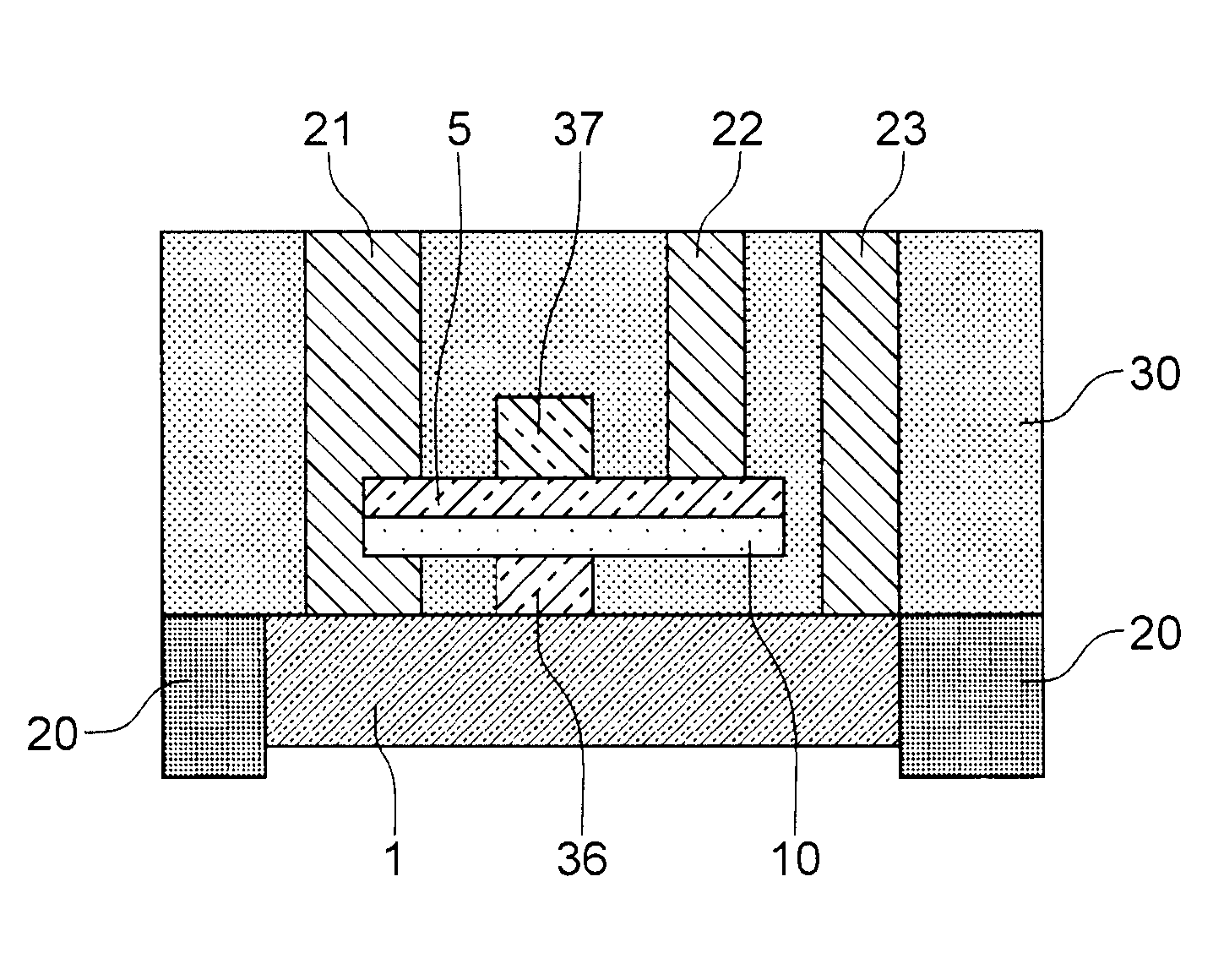
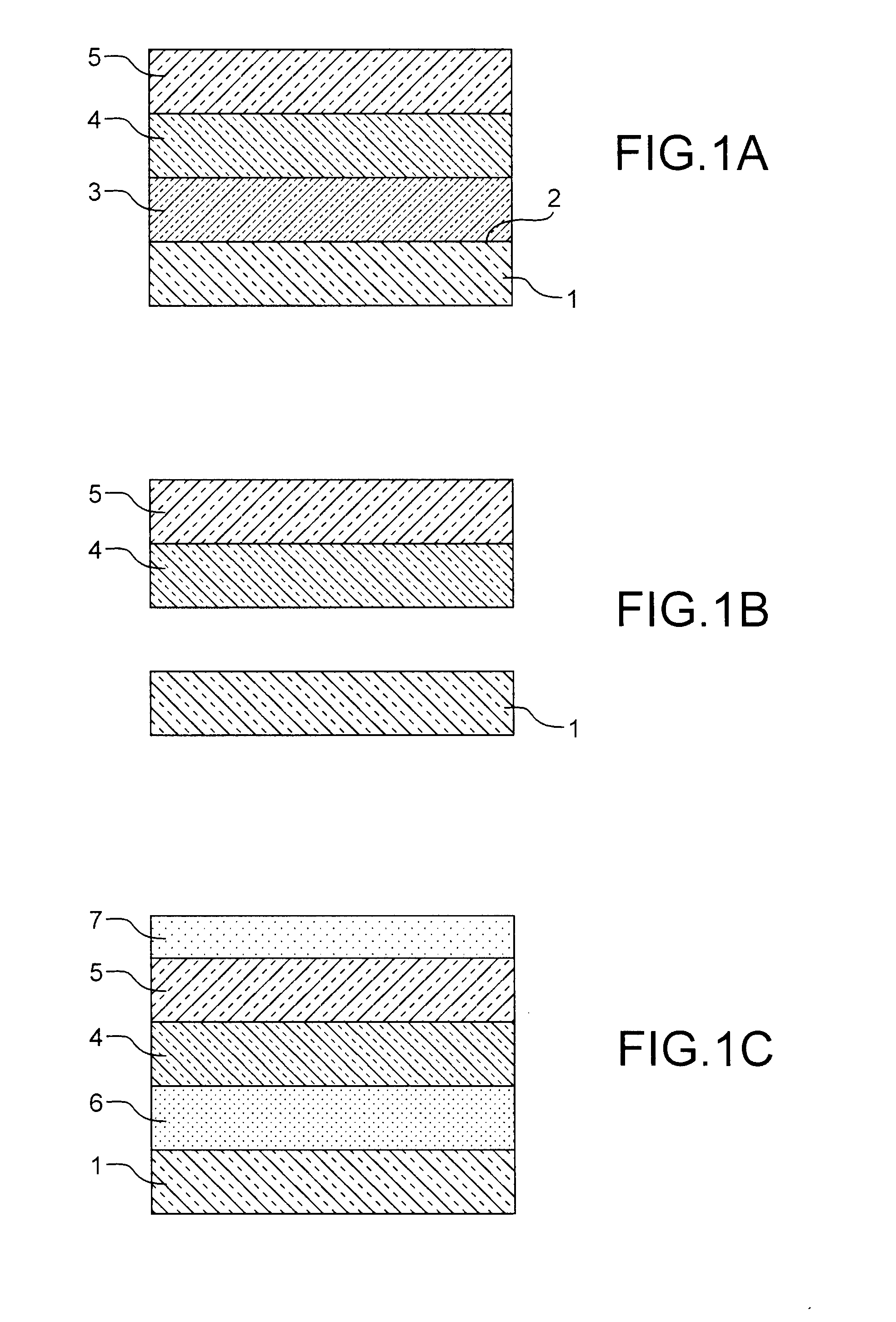
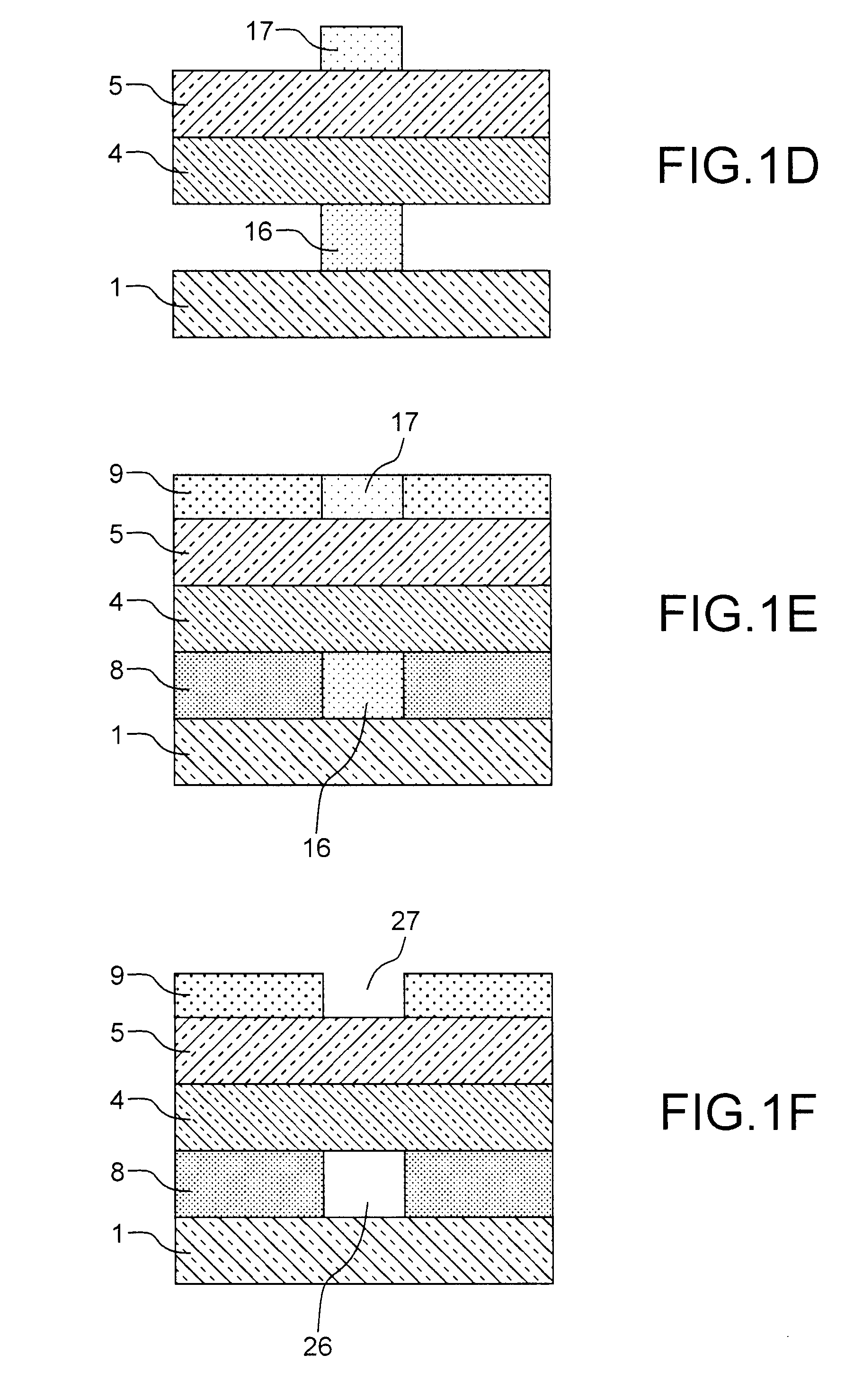
[0014]The present invention describes a method for stacking, on several levels (at least two), components that are self-aligned and electrically isolated from each other (semiconductors, microresonators, etc.) by an insulator layer. No method of recrystallisation of silicon, regrowth through a contact is necessary, thereby limiting the thermal budget constraints. The stacks are defined as of the first operation by epitaxy. Selective etchings and the use of self-aligned lithography then make it possible to work through the membrane.
[0015]The object of the invention is a method for producing stacked and self-aligned components on a substrate, comprising the following steps:
[0016]providing a...
PUM
| Property | Measurement | Unit |
|---|---|---|
| temperature | aaaaa | aaaaa |
| temperature | aaaaa | aaaaa |
| total pressure | aaaaa | aaaaa |
Abstract
Description
Claims
Application Information