Method of growing, on a dielectric material, nanowires made of semi-conductor materials connecting two electrodes

a technology of semi-conductor materials and nanowires, which is applied in the direction of nanotechnology, electrical equipment, and semiconductor devices, can solve the problems of large number of technological difficulties in the production of nanowires, inability to provide characteristics that match the requirements, and inability to achieve the quantum effects of field effect transistors no longer negligible, etc., and achieves limited heat budget and easy implementation.

Active Publication Date: 2012-01-03
COMMISSARIAT A LENERGIE ATOMIQUE ET AUX ENERGIES ALTERNATIVES +1
View PDF11 Cites 4 Cited by
  • Summary
  • Abstract
  • Description
  • Claims
  • Application Information

AI Technical Summary

Benefits of technology

[0009]The object of the invention is to provide a method for fabricating nanowires made of semi-conductor material of reproducible and perfectly well-defined diameter, this method being, easy to implement and having a limited heat budget.

Problems solved by technology

The transistors are now of nanometric size and production thereof is meeting with a large number of technological difficulties.
Quantum effects within the field effect transistor are no longer negligible and conventional microelectronics materials are no longer able to provide characteristics to match the required specifications.
This approach presents the drawback of requiring the use of conventional photolithography methods to define the dimensions of the nanowires and the use of a single-crystal silicon substrate to obtain single-crystal nanowires.
Furthermore, the clusters being annealed results in a large dispersion on the diameter of the nanowires.
These two approaches are incompatible with industrial integration of circuits comprising several levels of transistors one above the other.
Formation of a second layer of single-crystal silicon does in fact require the use of technological resolidification or layer transfer methods having thermal budgets that may be incompatible with the transistors formed on a first layer of silicon.
Nanowires do however present a large dispersion in their dimensions (diameter, width, thickness) from one nanowire to the other which makes use thereof in a semi-conductor circuit impossible.

Method used


Image

  • Method of growing, on a dielectric material, nanowires made of semi-conductor materials connecting two electrodes
  • Method of growing, on a dielectric material, nanowires made of semi-conductor materials connecting two electrodes

Examples


Embodiment Construction

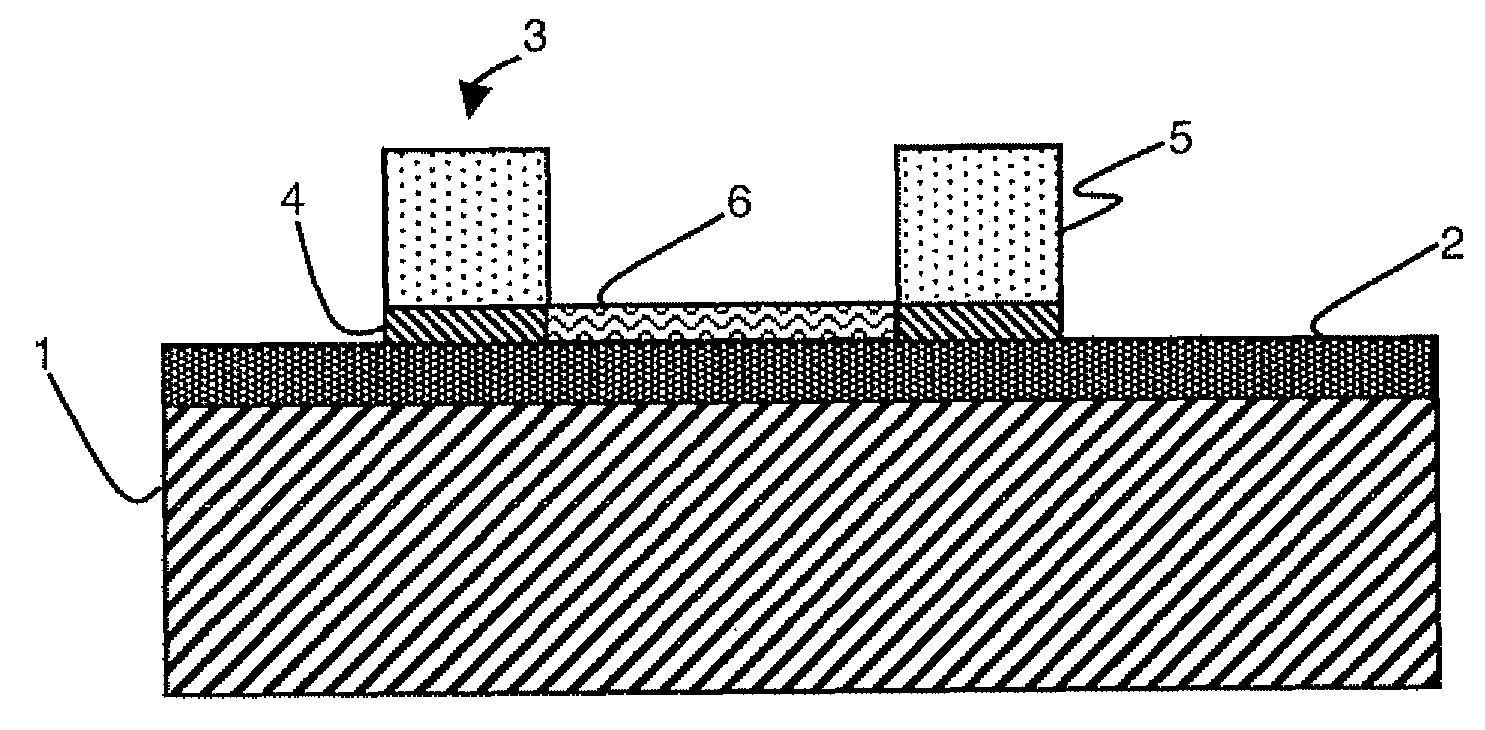
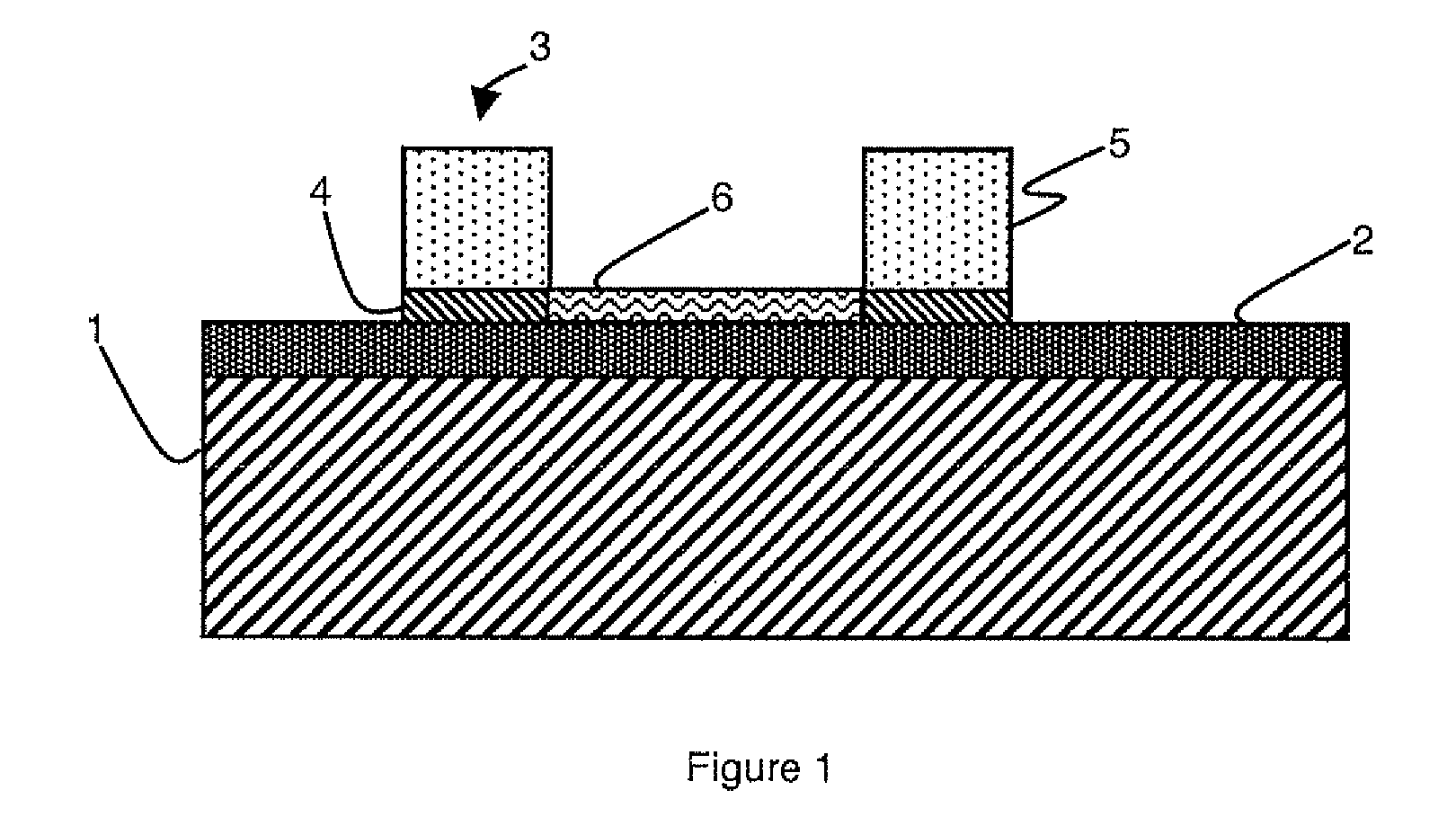
[0012]As illustrated in FIG. 1, two electrodes 3 made from metallic material are formed on a layer of dielectric material 2 of a substrate 1. Perpendicularly to substrate 1, electrodes 3 present substantially parallel opposite lateral surfaces (vertical in FIG. 1) between which the nanowires have to be formed.

[0013]Layer of dielectric material 2 is for example chosen from silicon oxide-based materials, silicon nitride-based materials, HfO2-based materials and Al2O3-based materials. Substrate 1 is for example made from bulk silicon, but it can be made from glass or from any other material able to withstand the subsequent technological steps. If substrate 1 is made from dielectric material, layer 2 can be integrated in substrate 1. Substrate 1 can for example comprise transistors forming integrated circuits encapsulated in layer of dielectric material 2.

[0014]A layer of catalyst material 4, in contact with layer of dielectric material 2, is formed by a bottom layer of at least one of ...


PUM

PropertyMeasurementUnit
pressureaaaaaaaaaa
temperatureaaaaaaaaaa
thicknessaaaaaaaaaa

Abstract

Electrodes made from metallic material are formed on a layer of dielectric material. A bottom layer of at least one of the electrodes constitutes a catalyst material in direct contact with the layer of dielectric material. Nanowires are grown by means of the catalyst, between the electrodes, parallel to the layer of dielectric material. The nanowires connecting the two electrodes are then made from single-crystal semi-conductor material and in contact with the layer of dielectric material.

Description

BACKGROUND OF THE INVENTION[0001]The invention relates to a method for producing nanowires connecting two electrodes, the nanowires being made from single-crystal semi-conductor material, the method successively comprising on a layer of dielectric material:[0002]formation of the electrodes,[0003]growth of the nanowires, by means of a catalyst, between the electrodes, parallel to the layer of dielectric material.STATE OF THE ART[0004]Continuous improvement of the performances of microelectronic circuits requires the integration density of the elementary components of the circuits to be increased. Up to now, improvement of performances was achieved by constant miniaturization of the dimensions of the MOSFET transistor. The transistors are now of nanometric size and production thereof is meeting with a large number of technological difficulties. Quantum effects within the field effect transistor are no longer negligible and conventional microelectronics materials are no longer able to ...

Claims


Application Information

Patent Timeline
Patent Type & Authority Patents(United States)
IPC IPC(8): H01L21/36
CPCB82Y10/00H01L21/02532H01L21/02603H01L21/02639H01L21/02645H01L29/0665H01L29/0673H01L21/0237H01L21/0262Y10S977/938
Inventor ERNST, THOMASBARON, THIERRYFERRET, PIERREGENTILE, PASCALSALEM, BASSEM
Owner COMMISSARIAT A LENERGIE ATOMIQUE ET AUX ENERGIES ALTERNATIVES
Why Eureka
Try Eureka