Liquid crystal display device and manufacturing method thereof

Active Publication Date: 2010-04-29
PANASONIC LIQUID CRYSTAL DISPLAY CO LTD +1
View PDF2 Cites 7 Cited by
  • Summary
  • Abstract
  • Description
  • Claims
  • Application Information

AI Technical Summary

Benefits of technology

[0030]To explain typical advantageous effects acquired by the present invention are as follows.
[0031]The liquid crystal filling port can be reliably sealed even when a size of a picture frame is made small.
[0032]The plural-piece manufacturing effi

Problems solved by technology

However, when the substrate is formed such that the substrate does not project from the sealing member for decreas

Method used


Image

  • Liquid crystal display device and manufacturing method thereof
  • Liquid crystal display device and manufacturing method thereof
  • Liquid crystal display device and manufacturing method thereof

Examples


Example

Embodiment 1

Schematic Constitution of the Whole Liquid Crystal Display Device

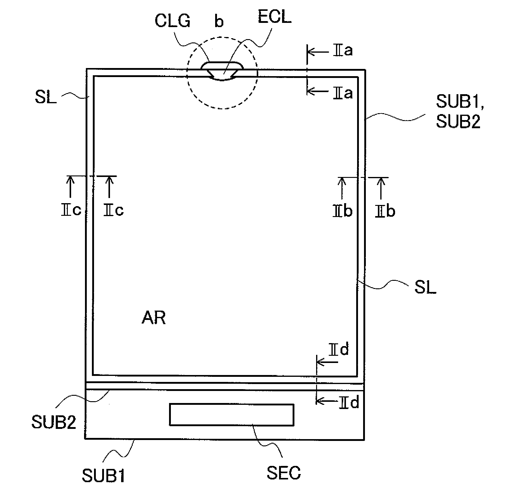
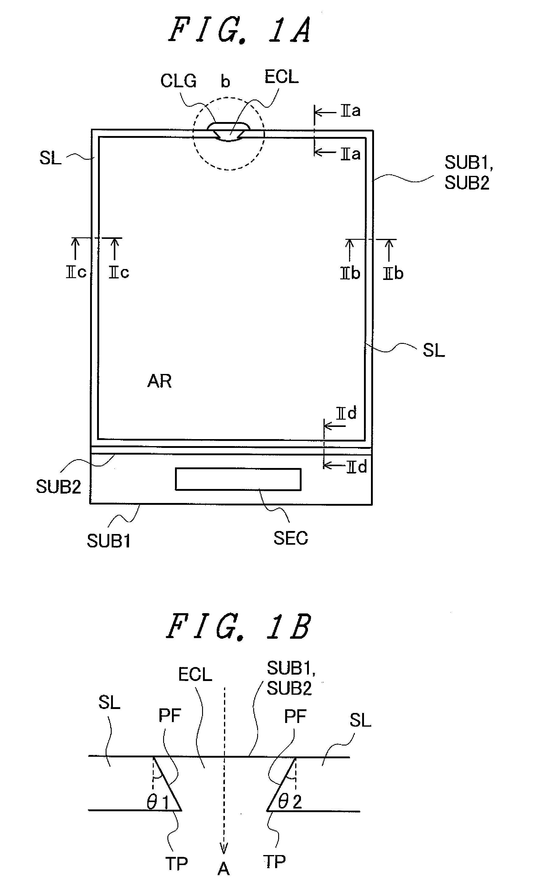
[0051]FIG. 1A is a schematic plan view showing an embodiment 1 of a liquid crystal display device of the present invention.

[0052]In FIG. 1A, for example, a substrate SUB1 and a substrate SUB2 which are made of glass are arranged to face each other in an opposed manner. Both the substrate SUB1 and the substrate SUB2 have a quadrangular shape (rectangular shape). An area of the substrate SUB2 is smaller than an area of the substrate SUB1 so that a side portion of the substrate SUB1 arranged on a lower side of the drawing, for example, is exposed. A semiconductor device (chip) SEC for driving pixels is mounted on the side portion of the substrate SUB1 with the semiconductor device SEC face down on the lower side in the drawing.

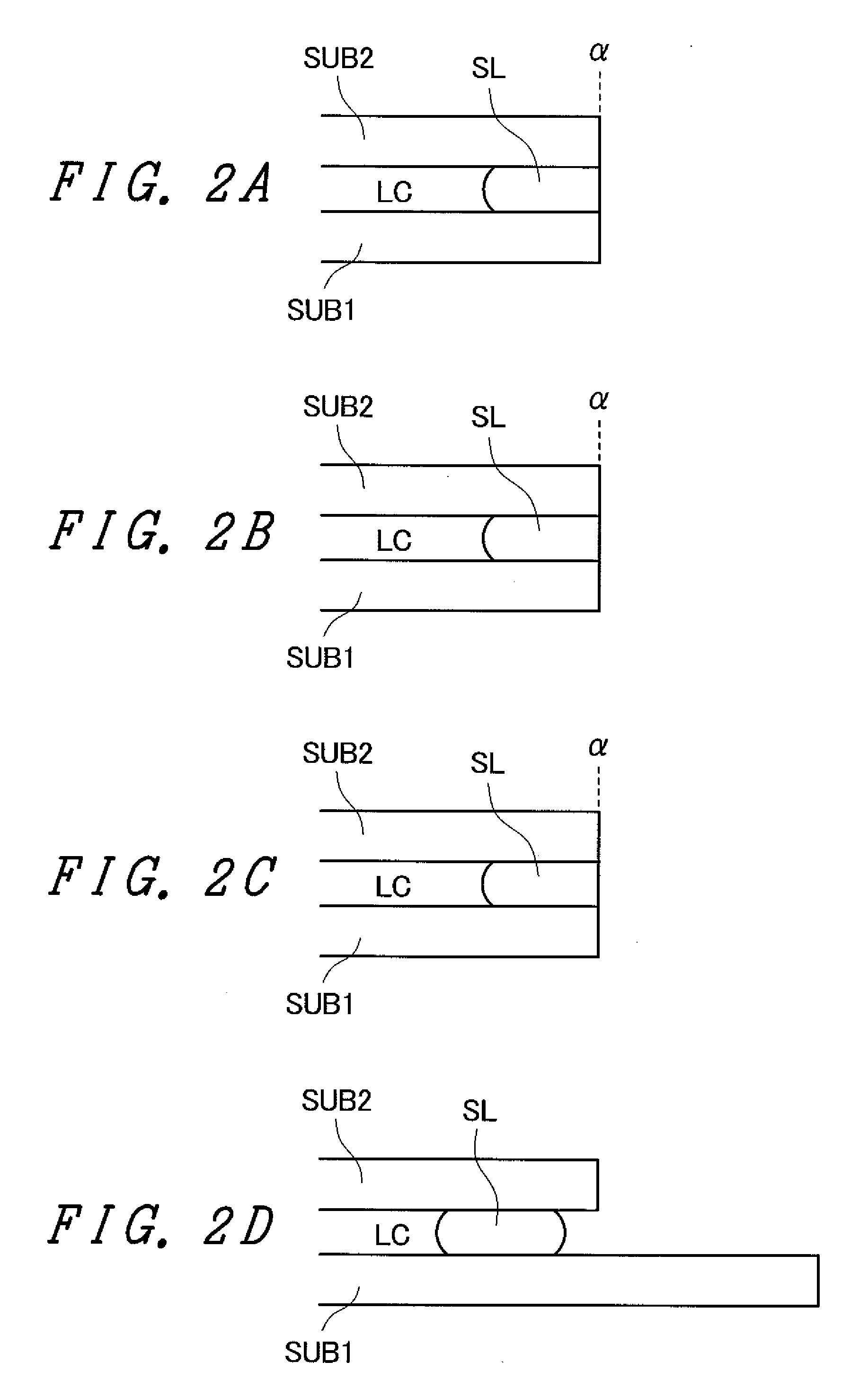
[0053]Liquid crystal LC (see FIG. 2A to FIG. 2D) is sandwiched between the substrate SUB1 and the substrate SUB2. The liquid crystal LC is sealed in a gap defined between the substrate S...

Example

Embodiment 2

[0071]FIG. 4A is a constitutional view showing an embodiment 2 of the liquid crystal display device of the present invention, and shows another constitution of the sealing member SL at a portion within a dotted-line frame b in FIG. 1A. Here, FIG. 4A shows a pattern of the sealing member SL after the substrate SUB1 and the substrate SUB2 are adhered to each other and a gap adjustment between the substrate SUB1 and the substrate SUB2 is made. In the state shown in FIG. 4A, the substrate SUB1 and the substrate SUB2 are not yet cut. In the drawing, a chained line P indicates a cut portion of the substrate SUB1 and the substrate SUB2. Accordingly, in FIG. 4A, the sealing member SL on a side of the drawing lower than the chained line P corresponds to the sealing member SL shown in FIG. 1B.

[0072]The constitution which makes the embodiment shown in FIG. 4A different from the embodiment shown in FIG. 1B lies in that the opposedly facing end portions TP of the sealing member SL at...

Example

Embodiment 3

[0076]FIG. 5A is a constitutional view showing an embodiment 3 of the liquid crystal display device of the present invention, and shows another constitution of the sealing member SL within the dotted-line frame b in FIG. 1A. FIG. 5A shows, in the same manner as the case shown in FIG. 4A, a pattern of the sealing member SL where the substrate SUB1 and the substrate SUB2 are adhered to each other and the gap adjustment between the substrate SUB1 and the substrate SUB2 is made but the substrate SUB1 and the substrate SUB2 is not yet cut from each other. In the drawing, a chained line P indicates a portion where the substrate SUB1 and the substrate SUB2 are cut.

[0077]In FIG. 5A, to respective opposedly-facing end portions TP of the sealing member SL which constitute the liquid crystal filling port ECL, a material layer ML made of a material different from a material of the sealing member SL is respectively connected. The material layers ML are formed simultaneously with the ...


PUM


Abstract

In an liquid crystal display device which includes: an image display part having a plurality of pixels; and a sealing member which is formed between the first substrate and the second substrate while surrounding the image display part and seals the liquid crystal therein, the sealing member includes a liquid crystal filling port which is formed by cutting away a portion of the sealing member, an side-wall edge surface of the first substrate and a side-wall edge surface of the second substrate are made coplanar with a side-wall edge surface of the sealing member along the extending direction of the sealing member on at least one side of the first substrate and the second substrate where the liquid crystal filling port is formed, and the liquid crystal filling port is formed such that a width of the liquid crystal filling port is narrowed along the liquid-crystal filling direction.

Description

CROSS-REFERENCE TO RELATED APPLICATION[0001]The present application claims priority from Japanese application JP 2008-275049 filed on Oct. 27, 2008, the content of which is hereby incorporated by reference into this application.BACKGROUND OF THE INVENTION[0002]1. Field of the Invention[0003]The present invention relates to a liquid crystal display device and a manufacturing method thereof, and more particularly to the improvement of a sealing-member structural portion which constitutes a portion of an envelope of the liquid crystal display device.[0004]2. Description of the Related Art[0005]An envelope of a liquid crystal display device is constituted of a pair of substrates which are arranged to face each other in an opposed manner with liquid crystal sandwiched therebetween and a sealing member which seals the liquid crystal in a space defined between these substrates.[0006]An image display part is formed in the envelope, and the image display part is constituted of a plurality of...

Claims


Application Information

Patent Timeline
IPC IPC(8): G02F1/1339G02F1/1341
CPCG02F1/1341G02F1/1339
Inventor SHIGEKURA, YUKARIYAMADA, YASUYUKIMIYAIRI, HIROSHI
Owner PANASONIC LIQUID CRYSTAL DISPLAY CO LTD
Why Eureka
Try Eureka