Semiconductor device having built-in self-test circuit and method of testing the same

a technology of self-testing and semiconductor devices, which is applied in the direction of measurement devices, instruments, computing, etc., can solve the problems of increasing the cost of testing lsis, the inability to reduce the testing time beyond a certain extent, and the difficulty in determining the timing of reading a fault detection signal from the parallel conversion circuit, so as to reduce the cost of testing and accurate determination

Inactive Publication Date: 2010-04-29
RENESAS ELECTRONICS CORP
View PDF14 Cites 9 Cited by
  • Summary
  • Abstract
  • Description
  • Claims
  • Application Information

AI Technical Summary

Benefits of technology

[0010]In recent years, LSIs have been remarkably growing in scale and operating speed. Keeping pace with the trend, the cost of testing LSIs has been increasing. Shortening the time required to test LSIs is one way of reducing the cost of testing LSIs. Namely, making it possible to successively test LSIs using a high-speed clock signal results in shortening the time required to test LSIs and reducing the cost of testing them.
[0016]According to the exemplary aspects, the marker pulse signal is generated before the generation of a test result signal, so that the timing for reading the test result signal can be accurately determined. It is therefore possible to successively perform checking with an expected value and faulty-cycle detection using a faster clock signal so as to reduce the cost of testing.

Problems solved by technology

Keeping pace with the trend, the cost of testing LSIs has been increasing.
It is therefore not possible to perform an error detection operation at every cycle of a clock signal, so that the testing time cannot be reduced beyond a certain extent.
When the clock signal is made faster, however, it becomes increasingly difficult to determine the timing for reading a fault detection signal from the parallel conversion circuit.
In this case, however, the delay time involved in reading the fault detection signal is dependent, for example, on the LSI structure and the wiring length between the tester and the LSI, so that it is not constant.
Therefore, when the clock signal is made faster, it becomes difficult to accurately determine the timing of the fault detection signal, so that performing the test becomes increasingly difficult.

Method used


Image

  • Semiconductor device having built-in self-test circuit and method of testing the same
  • Semiconductor device having built-in self-test circuit and method of testing the same
  • Semiconductor device having built-in self-test circuit and method of testing the same

Examples


first exemplary embodiment

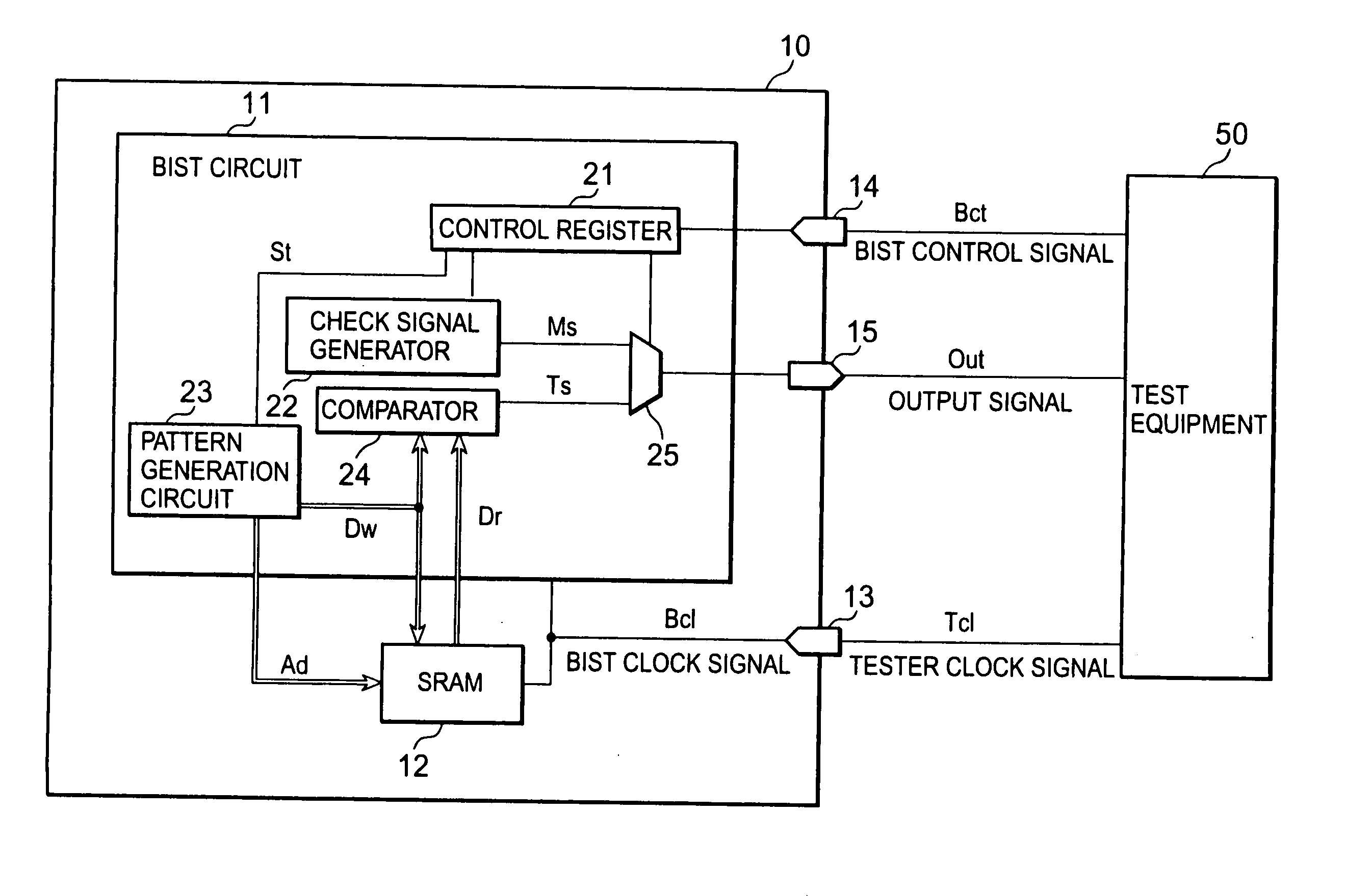
[0032]FIG. 1 is a block diagram showing a configuration of a semiconductor device according to a first exemplary embodiment of the present invention. Referring to FIG. 1, a semiconductor device 10 includes a BIST circuit 11, an SRAM 12, input terminals 13 and 14, and an output terminal 15. The BIST circuit includes a control register 21, a check signal generator 22, a pattern generation circuit 23, a comparator 24, and a selector 25.

[0033]The semiconductor device 10 has a tester clock signal Tc1 inputted thereto from an external test equipment 50 via the input terminal 13 and supplies the inputted tester clock signal Tc1 as a BIST clock signal Bc1 to the BIST circuit 11 and the SRAM 12. The BIST circuit 11 tests the SRAM 12 in synchronization with the BIST clock signal Bc1. The SRAM 12 reads and writes data used for the test in synchronization with the BIST clock signal Bc1.

[0034]The semiconductor device 10 has a BIST control signal Bct inputted thereto from the external test equipm...

second exemplary embodiment

[0048]FIG. 5 is a block diagram showing a configuration of a semiconductor device according to a second exemplary embodiment of the present invention. In FIG. 5, components identical to those shown in FIG. 1 are assigned the same reference numerals as in FIG. 1 and their descriptions are omitted. A semiconductor device 10a shown in FIG. 5 is like the semiconductor device 10 shown in FIG. 1 additionally including a PLL 16, a counter 17, and a serial / parallel converter 18.

[0049]The PLL 16 generates a BIST clock signal Bc1 by multiplying a tester clock signal Tc1 (by three in the present example) and supplies the BIST clock signal Bc1 thus generated to a BIST circuit 11, an SRAM 12, a counter 17, and a serial / parallel converter 18.

[0050]The counter 17 frequency-divides the BIST clock signal Bc1 (by three in the present example) and supplies the resultant signal as a collection signal Pei to the serial / parallel converter 18.

[0051]The serial / parallel converter 18 includes flip-flop circu...

third exemplary embodiment

[0054]FIG. 7 is a block diagram showing a configuration of a semiconductor device according to a third exemplary embodiment of the present invention. In FIG. 7, components identical to those shown in FIG. 1 are assigned the same reference numerals as in FIG. 1 and their descriptions are omitted. A semiconductor device 10b shown in FIG. 7 is like the semiconductor device 10 shown in FIG. 1 less the check signal generator 22 and the selector 25.

[0055]A pattern generation circuit 23b writes data for fault detection to an address to be a target of marker pulse generation of an SRAM 12. A comparator 24 detects the data for fault detection and outputs a marker pulse to a test result signal Ts. Namely, the control register 21b makes the pattern generation circuit 23b generate, before generating a test result signal, a prescribed marker pulse whose phase is the same as that of the test result signal. The test equipment 50 can accurately determine, like in the first exemplary embodiment, the...


PUM


Abstract

A semiconductor device includes circuits to be tested, an input terminal for receiving a tester clock signal from outside, a built-in self-test (BIST) circuit for logically testing the circuit at every cycle of a tester clock signal, and an output terminal for outputting a test result signal representing a result of testing performed in the BIST circuit. Before generating a test result signal, the BIST circuit generates a marker signal, whose phase is identical to the phase of the test result signal, instead of the test result signal.

Description

INCORPORATION BY REFERENCE[0001]This application is based upon and claims the benefit of priority from Japanese Patent Application No. 2008-274448 which was filed on Oct. 24, 2008, the disclosure of which is incorporated herein in its entirety by reference.BACKGROUND OF THE INVENTION[0002]1. Field of the Invention[0003]The present invention relates to a semiconductor device and a method of testing the same, and more particularly, to a semiconductor device having a built-in self-test circuit and a method of testing the same.[0004]2. Description of Related Art[0005]To make it easy to test semiconductor devices, semiconductor devices are each provided with a built-in self-test (BIST) circuit for detecting faults in them. Patent document 1 listed below, for example, discloses a semiconductor device having a BIST circuit which can identify a fail-data address and a fail-data bit without causing the testing time or cost to increase and which can easily test an AC characteristic, for examp...

Claims


Application Information

Patent Timeline
Patent Type & Authority Applications(United States)
IPC IPC(8): G01R31/3187G06F11/00
CPCG01R31/31727G01R31/31726
Inventor NAKAMURA, YOSHIHIRO
Owner RENESAS ELECTRONICS CORP
Why Eureka
Try Eureka