Crystalline solar cell having stacked structure and method of manufacturing the crystalline solar cell

a solar cell and crystalline technology, applied in the field of solar cells, can solve the problems of reducing electricity generation efficiency, recombination rate, and affecting the efficiency of solar energy generation, and achieve the effect of increasing light absorption efficiency

Inactive Publication Date: 2010-05-06
SILICONFILE TECH INC
View PDF1 Cites 1 Cited by
  • Summary
  • Abstract
  • Description
  • Claims
  • Application Information

AI Technical Summary

Benefits of technology

[0014]The present invention provides a crystalline solar cell having a stacked structure including a non-conductive lattice buffer layer that can remove lattice defects that may occur at the interface between solar cell layers having different band gaps and different lattice parameters from each other and electrically connect the solar cell layers to each other, thereby increasing light absorption efficiency.

Problems solved by technology

However, in a case where crystal growth of materials having different lattice parameters is performed in order to stack the solar cell layers, lattice defects occur due to a difference between the lattice parameters of the two materials for forming two solar cell layers, respectively, at the interface between the solar cell layers, and the generated lattice defects may operate as a recombination center between electron-hole.
This results in increase in a recombination rate and decrease in electricity generation efficiency.
However, the aforementioned method has complex processes and has a disadvantage in that lattice strain cannot be removed.
Therefore, there is a problem in that the TCO layer 120 cannot be used for the crystalline solar cell.
Therefore, although the method using the TCO layer 120 can be used for an amorphous solar cell, the method cannot be applied to the crystalline solar cell.

Method used


Image

  • Crystalline solar cell having stacked structure and method of manufacturing the crystalline solar cell
  • Crystalline solar cell having stacked structure and method of manufacturing the crystalline solar cell
  • Crystalline solar cell having stacked structure and method of manufacturing the crystalline solar cell

Examples


Embodiment Construction

[0023]Hereinafter, exemplary embodiments of the present invention will be described in detail with reference to the attached drawings.

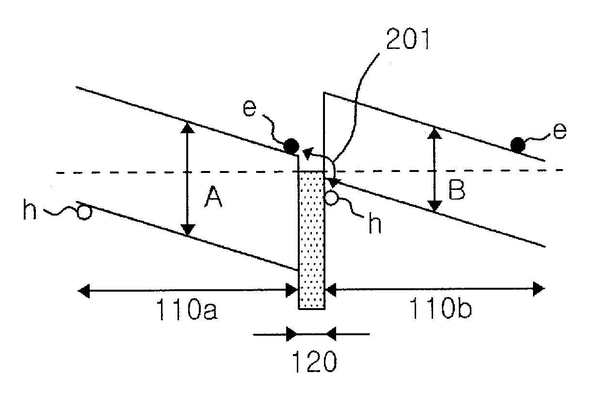
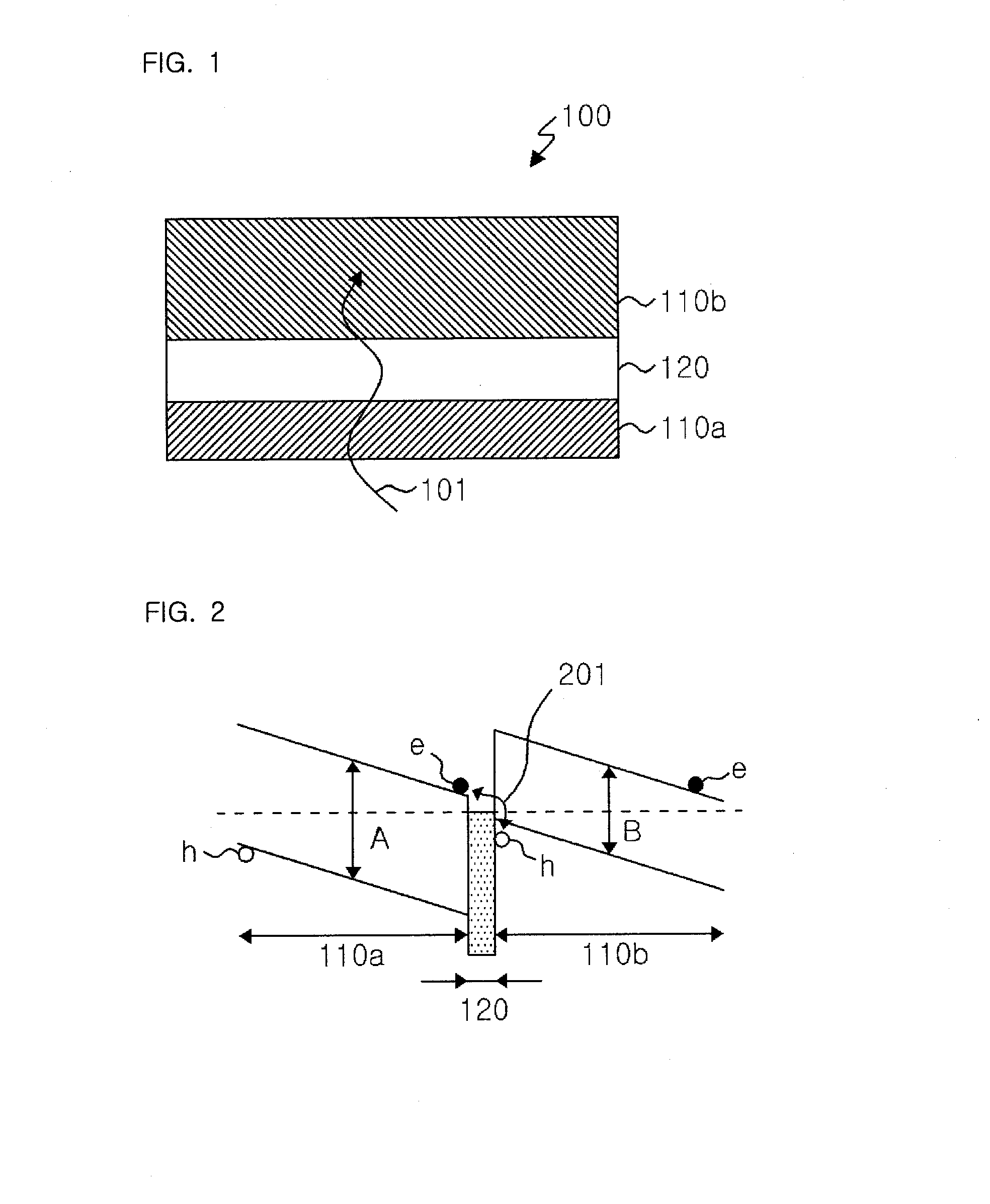
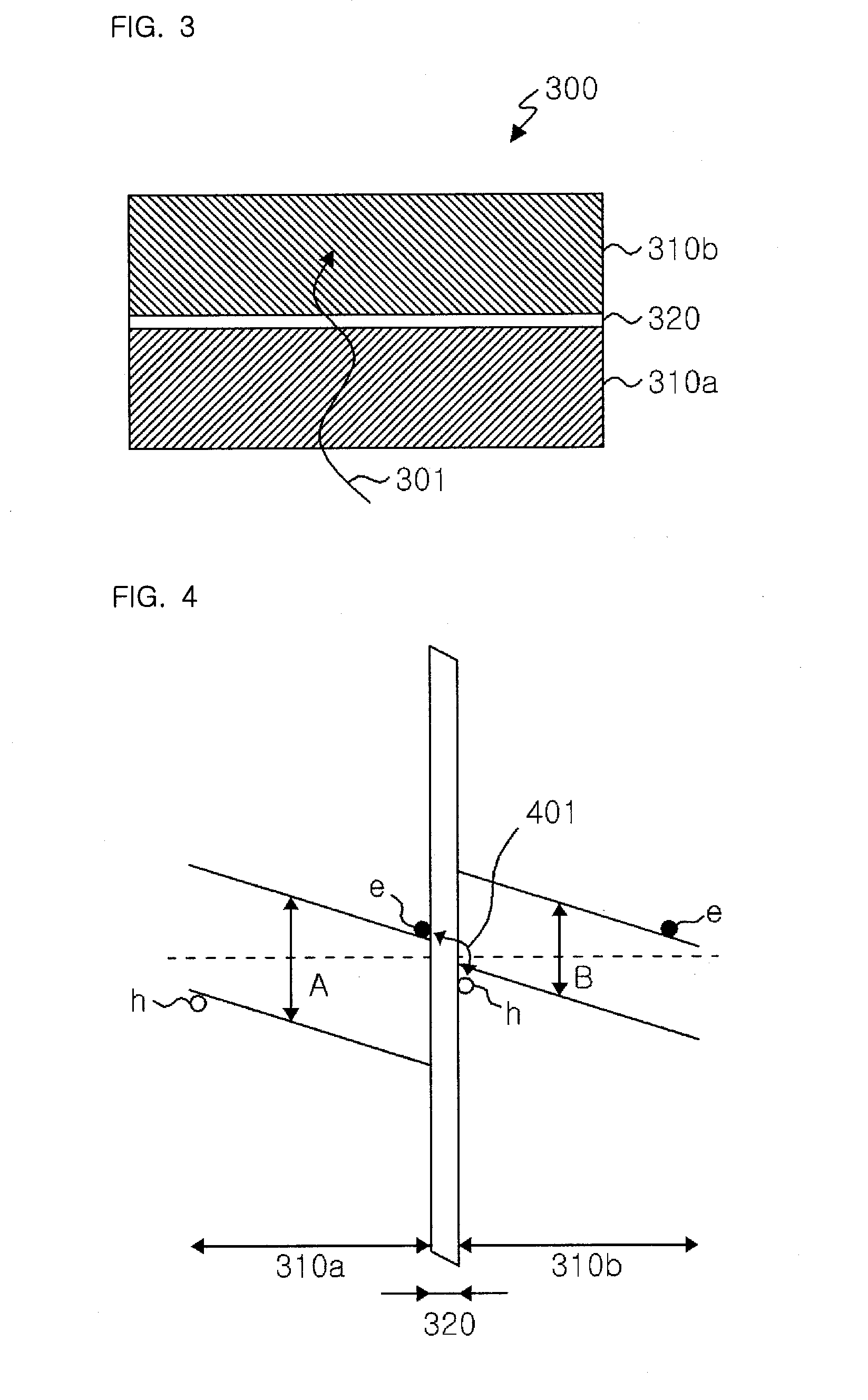
[0024]FIG. 3 illustrates a crystalline solar cell having a stacked structure according to an embodiment of the present invention. The crystalline solar cell 300 having a stacked structure illustrated in FIG. 3 includes a first solar cell layer 310a, a second solar cell layer 310b, and a non-conductive lattice buffer layer 320.

[0025]The crystalline first solar cell layer 310a is formed at a front surface in a direction 301 of incident light, and the crystalline second solar cell layer 310b is formed at a rear surface in the direction 301 of incident light. The non-conductive lattice buffer layer 320 is made of a non-conductive material and formed between the first and second solar cell layers 310a and 310b.

[0026]The first solar cell layer 310a first absorbs the incident light and may have a wide energy band of a relatively wider band gap A, and the se...


PUM


Abstract

Provided are a crystalline solar cell having a stacked structure capable of increasing light absorption efficiency and preventing deterioration in a semiconductor and a method of manufacturing the crystalline solar cell. The crystalline solar cell having a stacked structure includes a non-conductive lattice buffer layer which is made of a non-conductive material and formed between crystalline solar cell layers, wherein the non-conductive lattice buffer layer electrically connects the solar cell layers to each other by a tunneling effect. The method of manufacturing the crystalline solar cell includes steps of forming a crystalline first solar cell layer, forming a non-conductive lattice buffer layer using a non-conductive material on the first solar cell layer, and forming a crystalline second solar cell layer on the non-conductive lattice buffer layer.

Description

BACKGROUND OF THE INVENTION[0001]1. Field of the Invention[0002]The present invention relates to a solar cell, and more particularly, to a crystalline solar cell having a stacked structure with high light absorption efficiency.[0003]2. Description of the Related Art[0004]In general, it is well known that a solar cell having a stacked structure can absorb light in a very wide wavelength range and has high light absorption efficiency. For this, in the stacked structure of the solar cell, a solar cell layer having a wide band gap is disposed at a front surface on which light is incident and a solar cell layer having a narrow band gap is disposed at a rear surface on which the light incident later.[0005]FIG. 1 illustrates a solar cell having a conventional stacked structure. The solar cell 100 having the conventional stacked structure illustrated in FIG. 1 includes a first solar cell layer 110a which has a wide band gap A and is disposed at a front surface in a direction 101 of incident...

Claims


Application Information

Patent Timeline
Patent Type & Authority Applications(United States)
IPC IPC(8): H01L31/00H01L31/18
CPCH01L31/0687H01L31/18Y02E10/544Y02P70/521Y02P70/50H01L31/047
Inventor LEE, BYOUNG-SU
Owner SILICONFILE TECH INC
Why Eureka
Try Eureka