

Method of forming multiple nanopatterns and method of manufacturing organic solar cell using the same
a technology of organic solar cells and nano-patterns, applied in the field of multiple nano-patterns and a manufacturing method of organic solar cells, can solve the problems of increasing processing costs and achieve the effect of increasing light absorption efficiency and low cos
- Summary
- Abstract
- Description
- Claims
- Application Information
AI Technical Summary
Benefits of technology
Problems solved by technology
Method used
Image

Examples
preparation example 1
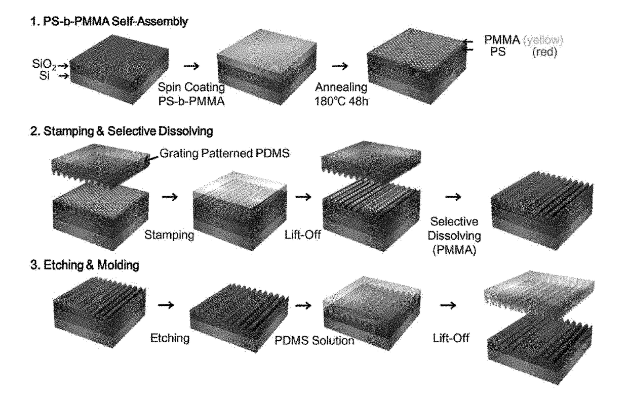
Nanopattern (Grating Pattern)
[0089]Polystyrene (Mn(PS)=192,000 g mol−1, Aldrich) was dissolved in an amount of 2 wt % in toluene to give a polystyrene solution, which was then applied through spin coating to a thickness of about 70 nm on a silicon wafer. Next, thermal treatment was conducted in a vacuum oven at 130° C. for 2 hr, thus forming a polystyrene layer. A polydimethylsiloxane (PDMS) precursor solution (comprising a curing agent and a silicon elastic polymer at a mass ratio of 1:10) was poured on a grating mold (Thorlabs, GH13-36U, Periodicity=278 nm) and cured at 60° C. for 2 hr, thus forming a nanoimprinting stamp. The nanoimprinting stamp was placed on the thermally treated polystyrene layer and pressure was applied at 130° C. for 10 min to thus transfer the grating nanopattern, thus preparing a grating-nanopatterned polystyrene layer.
[0090]Using the grating-nanopatterned polystyrene layer as a mask, reactive ion dry etching (RIE) (TTL Dielectric RIE, CF4 / CHF3 / O2 / Ar, flow...
preparation example 2
Pattern (Nanopost Pattern)
[0092]Polystyrene-block-polymethylmethacrylate (PS-b-PMMA, Mn(PS)=57,000 g mol−1, Mn(PMMA)=25,000 g mol−1, Mw / Mn<1.2, Aldrich) was dissolved in an amount of 2 wt % in toluene to give a block copolymer solution, which was then applied through spin coating to a thickness of about 70 nm on a silicon wafer. Next, thermal treatment was conducted in a vacuum oven at 180° C. for 48 hr, thus forming a phase-separated block copolymer layer. Subsequently, the phase-separated block copolymer layer was irradiated with UV light for 30 min and immersed in acetic acid for 20 min to selectively remove PMMA, thereby forming a nanopost-patterned polystyrene layer.
[0093]Thereafter, the preparation of a nanopost-patterned silicon wafer using the nanopost-patterned polystyrene layer as a mask and the preparation of a nanopost-patterned stamp using the nanopost-patterned silicon wafer were carried out in the same manner as in Preparation Example 1.
example 1
of Double Nanopattern (Multiple Patterns)
[0094]Polystyrene-block-polymethylmethacrylate (PS-b-PMMA, Mn(PS)=57,000 g mol−1, Mn(PMMA)=25,000 g mol−1, Mw / Mn<1.2, Aldrich) was dissolved in an amount of 2 wt % in toluene to give a block copolymer solution, which was then applied through spin coating to a thickness of about 70 nm on a silicon wafer. Next, thermal treatment was conducted in a vacuum oven at 180° C. for 48 hr, thus forming a phase-separated block copolymer layer. Subsequently, a polydimethylsiloxane (PDMS) precursor solution (comprising a curing agent and a silicon elastic polymer at a mass ratio of 1:10) was poured on a grating mold (Thorlabs, GH13-36U, Periodicity=278 nm) and cured at 60° C. for 2 hr, thus forming a nanoimprinting stamp. The nanoimprinting stamp was placed on the phase-separated block copolymer layer, and pressure was applied at 130° C. for 10 min to thus transfer the grating pattern, followed by UV irradiation for 30 min and then immersion in acetic acid...
PUM
 Abstract
Description
Claims
Application Information