Method of manufacturing semiconductor device

Inactive Publication Date: 2010-05-06
SHINKO ELECTRIC IND CO LTD
View PDF7 Cites 0 Cited by
  • Summary
  • Abstract
  • Description
  • Claims
  • Application Information

AI Technical Summary

Benefits of technology

[0022]Exemplary embodiments of the present invention provide a method of manufacturing a semiconductor device, capable of suppressing a peeling that is caused due to a cutting at a boundary between a semiconductor substrate and an insulating layer.
[0028]According to the disclosed method, it is possible to provide the method of manufacturing the semiconductor device, capable of suppressing the peeling that is caused due to the cutting at the boundary between the semiconductor substrate and the insulating layer.

Problems solved by technology

However, in the semiconductor device 100 in the related art, the adhesion between the semiconductor substrate 110 and the insulating layer 103 is poor because their physical properties are different mutually.

Method used


Image

  • Method of manufacturing semiconductor device
  • Method of manufacturing semiconductor device
  • Method of manufacturing semiconductor device

Examples


first embodiment

Variation 2 of First Embodiment

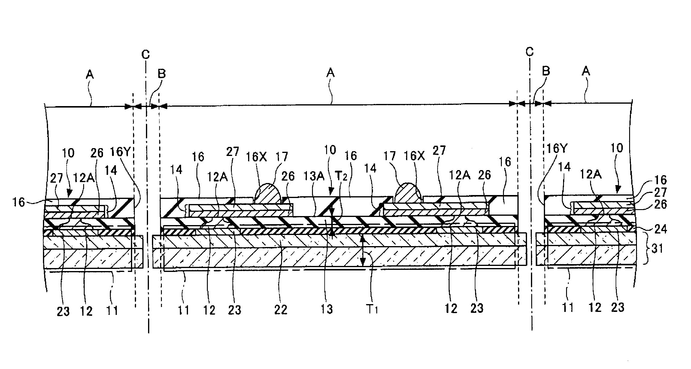
[0081]In steps shown in FIG. 22 of the first embodiment, individual piece like cover layers 33, each size of which corresponds to the semiconductor chip forming area A, may be pasted onto respective semiconductor chip forming areas A instead of the formation of the cover layer 29 to cover the whole upper surface (the upper surface 13A of the insulating layer 13 and the wiring patterns 14) of the structure shown in FIG. 21.

[0082]In a variation 2 of the first embodiment, manufacturing steps when the individual piece-like cover layers 33 are employed instead of the cover layer 29 will be explained hereunder. FIG. 32 to FIG. 35 are views showing steps of a variation 2 of the first embodiment of the present invention. In FIG. 32 to FIG. 35, the same reference symbols are affixed to the same constituent portions as those in FIG. 14 to FIG. 29 and in some cases their explanation is omitted herein.

[0083]At first, after the steps similar to those in FIG. 14 to ...


PUM


Abstract

A semiconductor substrate has a plurality of semiconductor chip forming areas and scribe areas including substrate cutting positions arranged between the plurality of semiconductor chip forming areas. An insulating layer having first opening portions, which expose all or a part of the scribe areas respectively, is formed on the semiconductor substrate. A solder resist layer having second opening portions, which expose all or a part of the scribe areas respectively, is formed on the insulating layer. Portions of the semiconductor substrate corresponding to the substrate cutting positions are cut.

Description

[0001]This application claims priority to Japanese Patent Application No. 2008-280171, filed Oct. 30, 2008, in the Japanese Patent Office. The Japanese Patent Application No. 2008-280171 is incorporated by reference in its entirety.TECHNICAL FIELD[0002]The present disclosure relates to a method of manufacturing a semiconductor device, including a step of forming an insulating layer on a semiconductor substrate and a step of cutting the semiconductor substrate.RELATED ART[0003]Out of the semiconductor devices in the related art, there is the semiconductor device that is called the chip-size package whose size is substantially identical to the semiconductor chip when viewed from the top (see FIG. 1, for example).[0004]FIG. 1 is a sectional view showing the semiconductor device in the related art. By reference to FIG. 1, a semiconductor device 100 in the related art includes a semiconductor chip 101, internal connection terminals 102, an insulating layer 103, wiring patterns 104, a sol...

Claims


Application Information

Patent Timeline
IPC IPC(8): H01L21/78
CPCH01L21/78H01L2224/13H01L2224/0554H01L2924/00014H01L2224/05571H01L2224/05624H01L2224/05573H01L2224/0557H01L2224/05599H01L2224/0555H01L2224/0556
Inventor KAZAMA, TAKUYA
Owner SHINKO ELECTRIC IND CO LTD
Why Eureka
Try Eureka