
Bonded body and insulating circuit substrate

Active Publication Date: 2020-10-08
MITSUBISHI MATERIALS CORP
View PDF0 Cites 0 Cited by
  • Summary
  • Abstract
  • Description
  • Claims
  • Application Information

AI Technical Summary

Benefits of technology

The invention provides a way to join ceramic and copper materials together without peeling, even when using ultrasonic waves. This results in a stronger bond that is useful for making insulating circuit substrates.

Problems solved by technology

Since this TiN layer is hard and brittle, there is a concern that cracks may be generated in the ceramic substrate during loading of a thermal cycle.

Method used


Image

  • Bonded body and insulating circuit substrate
  • Bonded body and insulating circuit substrate
  • Bonded body and insulating circuit substrate

Examples


first embodiment

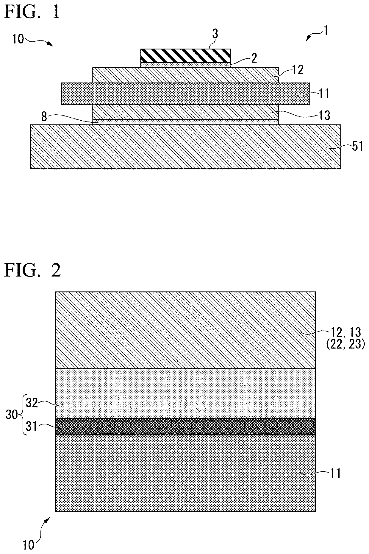
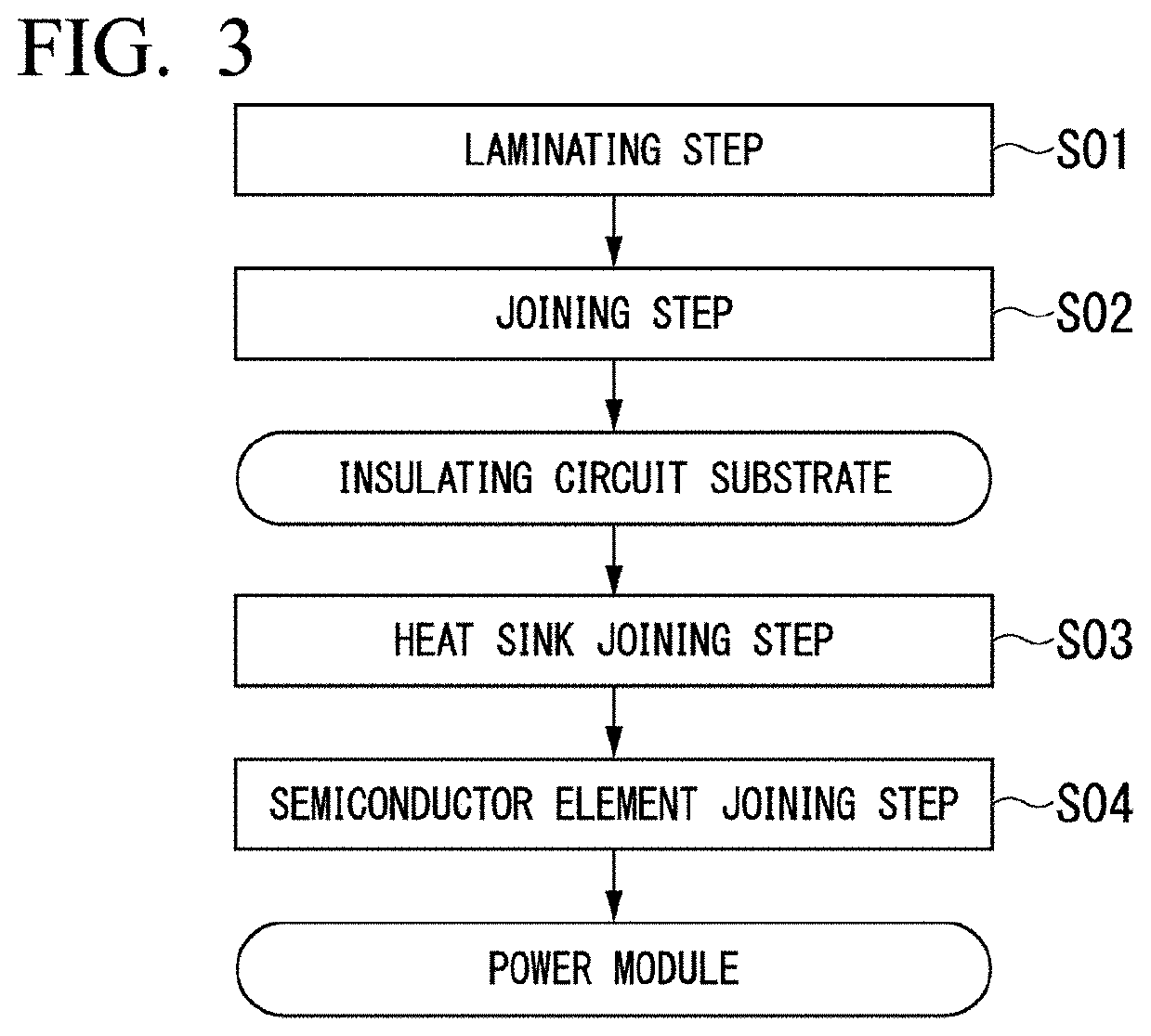
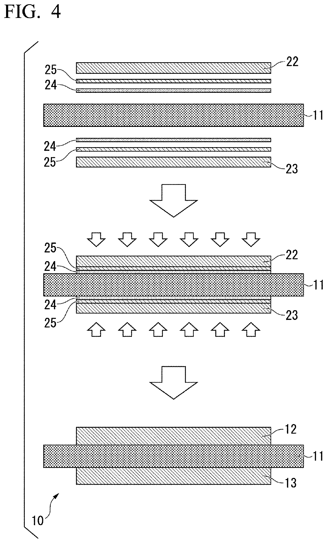
[0040]A description will be given below of a first embodiment of the present invention with reference to FIG. 1 to FIG. 4.

[0041]The bonded body according to the embodiment of the present invention is an insulating circuit substrate 10 configured by joining a ceramic substrate 11 as a ceramic member formed of Si-based ceramics and a copper sheet 22 (circuit layer 12) as a copper member formed of copper or a copper alloy. Here, the Si-based ceramics refer to ceramics formed of a compound including an Si element.

[0042]FIG. 1 shows the insulating circuit substrate 10 which is an embodiment of the present invention and a power module 1 using the insulating circuit substrate.

[0043]The power module 1 is provided with the insulating circuit substrate 10, a semiconductor element 3 joined via a first solder layer 2 to one side (upper side in FIG. 1) of the insulating circuit substrate 10, and a heat sink 51 arranged via a second solder layer 8 on the other side (the lower side in FIG. 1) of t...

second embodiment

[0092]Next, a description will be given of a second embodiment of the present invention. In addition, the same reference numerals are used in the description where the configuration is the same as the first embodiment and detailed description thereof is omitted.

[0093]FIG. 5 shows a power module 101 provided with an insulating circuit substrate 110 according to the second embodiment of the present invention.

[0094]The power module 101 is provided with the insulating circuit substrate 110, the semiconductor element 3 joined via the solder layer 2 to one surface (the upper surface in FIG. 5) of the insulating circuit substrate 110, and the heat sink 51 joined to a lower side of the insulating circuit substrate 110.

[0095]As shown in FIG. 8, a circuit layer 112 is formed to configured to join a copper sheet 122 formed of copper or a copper alloy to one surface of the ceramic substrate 11. In the present embodiment, a rolled plate of oxygen-free copper is used as the copper sheet 122 formi...

example 1

[0136]A copper sheet (6 mm×6 mm×0.3 mm thickness) formed of oxygen-free copper is sequentially laminated using a brazing material and an active metal material described in Table 1 on one surface of a ceramic substrate (26 mm×26 mm×0.32 mm thickness) formed of the material shown in Table 1 to form a laminate.

[0137]Then, the laminate was put into a vacuum heating furnace in a state of being pressed under the load shown in Table 2, and heated to join a copper sheet to one surface of the ceramic substrate. The heating temperature and time were as shown in Table 2.

[0138]In the manner described above, the joint bodies of the Examples of the present invention and the Comparative Examples were obtained. For the obtained joint bodies, the “Material and Crystallinity of Active Metal Compound Layer” and the “Ultrasonic Wave Joining Property” were evaluated.

[0139](Material and Crystallinity of Active Metal Compound Layer)

[0140]Measurement was carried out using a transmission electron microscope...


PUM

PropertyMeasurementUnit
Thicknessaaaaaaaaaa
Thicknessaaaaaaaaaa
Temperatureaaaaaaaaaa

Abstract

A bonded body is formed to configured to join a ceramic member formed of a Si-based ceramic and a copper member formed of copper or a copper alloy, in which, in a joint layer formed between the ceramic member and the copper member, a crystalline active metal compound layer formed of a compound including an active metal is formed on the ceramic member side.

Description

TECHNICAL FIELD[0001]The present invention relates to a bonded body, which is formed to configured to join a ceramic member and a copper member, and an insulating circuit substrate provided with the bonded body.[0002]This application claims the priority of Japanese Patent Application No. 2017-213155 filed in Japan on Nov. 2, 2017 and Japanese Patent Application No. 2018-204040 filed in Japan on Oct. 30, 2018, the contents of which are incorporated herein.BACKGROUND ART[0003]Semiconductor devices such as LEDs or power modules have a structure in which a semiconductor element is joined on a circuit layer formed of a conductive material.[0004]Power semiconductor elements for controlling large amounts of power used for controlling wind power generation, electric vehicles, hybrid vehicles, and the like generate large amounts of heat and therefore, insulating circuit substrates, which are, for example, provided with a ceramic substrate formed of Si3N4 (silicon nitride), or the like and a ...

Claims


Application Information

Patent Timeline
IPC IPC(8): H01L23/373H05K1/09H05K1/03H05K3/46H05K3/34H05K1/02
CPCH05K1/09H01L23/3736H05K1/0271H05K3/4644H05K1/0306H05K3/341H01L23/3731H01L2224/32225C22C9/00C22C9/02C22C9/06H01L23/3735C04B2237/407C04B2237/368C04B2237/704C04B2237/706C04B37/026C04B2237/124C04B2237/126C04B2237/122C04B2237/708C04B35/645C04B2235/6581C04B2235/6562C04B2235/6567C04B2237/72C04B2237/068C04B2237/60C04B2237/402C04B2237/121C04B2237/128C04B2237/08B23K26/364B23K26/402B23K2103/54B23K2103/50B23K2103/42B23K1/0016B23K1/008B23K1/19B23K1/20B23K20/026B23K20/233B23K20/26B23K20/16B23K2101/42B23K2103/12B23K2103/56B23K2103/18B23K35/302B23K35/007C04B37/02B23K1/00H01L23/12H01L23/36B23K35/26B23K35/28B23K35/30C22C13/00C22C21/00
Inventor TERASAKI, NOBUYUKI
Owner MITSUBISHI MATERIALS CORP
Learn More