Switched charge storage element network

a technology of storage element network and charge storage element, applied in the field of switching charge storage element network, can solve the problems of large silicon area consumption, continuous time modulator clock jitter sensitivity limitation, rise/fall transient of feedback dac, etc., and achieve the effect of avoiding convolution of supply nois

Active Publication Date: 2010-05-13
STMICROELECTRONICS INT NV
View PDF5 Cites 2 Cited by
  • Summary
  • Abstract
  • Description
  • Claims
  • Application Information

AI Technical Summary

Benefits of technology

[0027]In accordance with another aspect of the present disclosure, a method for avoiding convolution of supply noise with a clock signal in a switched charge storage element integrator is provided, the method including periodically coupling a first switched charge storage element block to an inverting terminal of the integrator; and coupling a second switched charge storage element block to the inverting terminal for the duration for which the first switched charge storage element block is decoupled from the inverting terminal.

Problems solved by technology

However, discrete time modulators being sampled data systems require an anti-aliasing filter, which consumes substantial amount of silicon area.
However, continuous time modulators suffer from limitations of clock jitter sensitivity and rise / fall transients of feedback DAC.

Method used


Image

  • Switched charge storage element network
  • Switched charge storage element network
  • Switched charge storage element network

Examples


Embodiment Construction

[0041]The embodiments of the present disclosure are described in detail with reference to the accompanying drawings. However, the present disclosure is not limited to these embodiments which are only provided to explain more clearly the present disclosure to one of ordinary skill in the art of the present disclosure. In the accompanying drawings, like reference numerals are used to indicate like components.

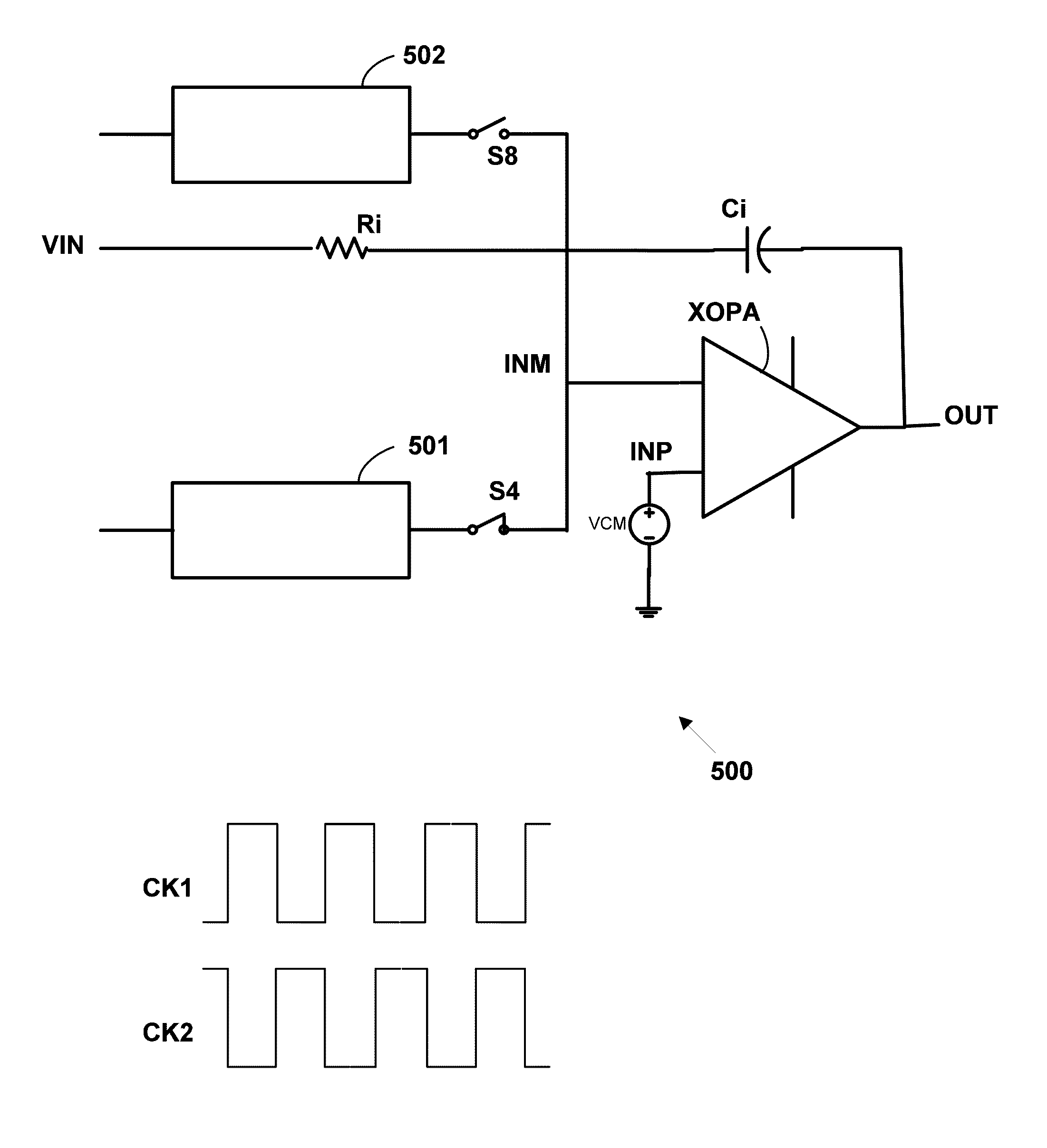
[0042]The present disclosure provides a switched charge storage element integrator in continuous or discrete time circuits. The integrator prevents fold back of the wide band supply noise in the single ended implementation of a continuous time integrator with a discrete time feedback DAC. A dummy switched charge storage element branch is added so as to make the supply noise continuous and eliminate its dependency on the clock phases, thereby zeroing its convolution with the clock.

[0043]The present disclosure also provides a switched charge storage element integrator. The switched ...


PUM


Abstract

A switched charge storage element integrator in a continuous or discrete time circuit, the integrator including a differential input amplifier, a first 2-terminal charge storage element, a second 2-terminal charge storage element, and a plurality of controlled switches. The differential input amplifier is coupled to a capacitor and a resistor and configured as an inverting integrator. An inverting terminal of the amplifier is coupled to two controlled switches. A non-inverting terminal of the amplifier is coupled to a reference voltage. The first and second switched charge storage element blocks are alternatingly coupled to the inverting terminal INM of the amplifier XOPA during the active state of a second clock signal and a first clock signal, respectively, for making the supply noise continuous and eliminating its dependency on the clock phases, thereby zeroing its convolution with the clock signal.

Description

BACKGROUND[0001]1. Technical Field[0002]The present disclosure relates to the field of switched charge storage element networks and, more specifically, to switched charge storage element integrators.[0003]2. Description of the Related Art[0004]Switched charge storage element networks i.e., switched capacitor networks are widely used to perform several functions. One application of a switched capacitor network is sigma delta modulators. Sigma delta modulators encode high resolution signals into low resolution signals using pulse-density modulation, and they are used in various modern electronic devices, such as analog-to-digital and digital-to-analog converters, frequency synthesizers, switched-mode power supplies, and motor controls. There are predominantly two approaches for realizing sigma delta modulators, namely, discrete time architecture and continuous time architecture. Discrete time modulators have some advantages over their continuous time counterparts in terms of robustnes...

Claims


Application Information

Patent Timeline
Patent Type & Authority Applications(United States)
IPC IPC(8): G06G7/18
CPCG06G7/18
Inventor DEBNATH, CHANDRAJITRANGBULLA, ANUBHUTI
Owner STMICROELECTRONICS INT NV
Why Eureka
Try Eureka