Eureka AIR delivers breakthrough ideas for toughest innovation challenges, trusted by R&D personnel around the world.

Laminated ceramic electronic component

Active Publication Date: 2010-05-13
MURATA MFG CO LTD
View PDF19 Cites 33 Cited by
  • Summary
  • Abstract
  • Description
  • Claims
  • Application Information

AI Technical Summary

Benefits of technology

[0019]According to a preferred embodiment of the present invention, the substantially rounded corners are preferably arranged on the boundaries between the end surfaces and the principal surfaces of the ceramic element assembly and the plating films forming the external terminal electrodes are arranged so that the ends stop at the corners. Thus, the distance from the ends of the plating films to the exposed portions of the internal conductors on the end surfaces of the ceramic element assembly can be sufficiently increased. Therefore, the penetration path of moisture or the like reaching the inside of the ceramic element assembly from the outside through the internal conductors can be relatively increased. Thus, the humidity resistance reliability of the laminated ceramic electronic component can increase.
[0020]Moreover, according to a preferred embodiment of the present invention, the plating films are arranged so as not to project from the principal surfaces in the lamination direction of the ceramic layer. Thus, the reduction in the thickness of the laminated ceramic electronic component can be advantageously achieved.
[0021]According to a preferred embodiment of the present invention, when the external terminal electrodes are further provided with the auxiliary conductor films arranged so as to extend up to one portion of the principal surfaces, so that the auxiliary conductor films cover the ends of the plating films, the humidity resistance reliability described above can further increase. The ends of the plating films are arranged so as to stop at the corners as described above, and thus only the auxiliary conductor films are provided as the external terminal electrodes on the principal surfaces. Therefore, an increase in the dimension in the height direction of the laminated ceramic electronic component can be kept to a minimum.
[0022]According to a preferred embodiment of the present invention, when the auxiliary conductor films described above include a glass component and the glass component partially penetrates in the interfaces of the plating films and the ceramic element assembly, the humidity resistance reliability can further increase.
[0023]According to a preferred embodiment of the present invention, when the internal conductors include dummy internal conductors, the fixing force of the plating films to the ceramic element assembly can increase and, simultaneously, by selecting the formation position of the dummy internal conductors, the precipitation areas of the plating films can be easily controlled.

Problems solved by technology

However, as the thickness of the ceramic layer has been increasingly reduced, short circuiting between internal electrodes is likely to occur, causing a problem in that it is difficult to secure the quality.
Therefore, there is a limitation on increasing the effective area of the internal electrodes.
However, there is a limitation on increasing the area of the ceramic layer within a determined standard dimension and, moreover, the thickness of the external terminal electrode itself also serves as a hindrance.
However, according to the method, the conductive paste is likely to thickly adhere to the center of the end surfaces of the ceramic element assembly due to the viscosity of the conductive paste.
However, the first typical example and the second typical example have problems to be solved.
First, in the first typical example, the distance from the ends of the plating films to the exposed portions of the internal electrodes is relatively short.
Thus, a penetration path of moisture or the like from the outside to the inside of the ceramic element assembly through the internal electrodes becomes short, and thus sufficient humidity resistance reliability cannot be obtained in some cases.
In contrast, in the second typical example, the plating film is formed while projecting from the principal surface of the ceramic element assembly, causing a problem of impeding the reduction in the thickness of laminated ceramic electronic components.

Method used


Image

  • Laminated ceramic electronic component
  • Laminated ceramic electronic component
  • Laminated ceramic electronic component

Examples


Embodiment Construction

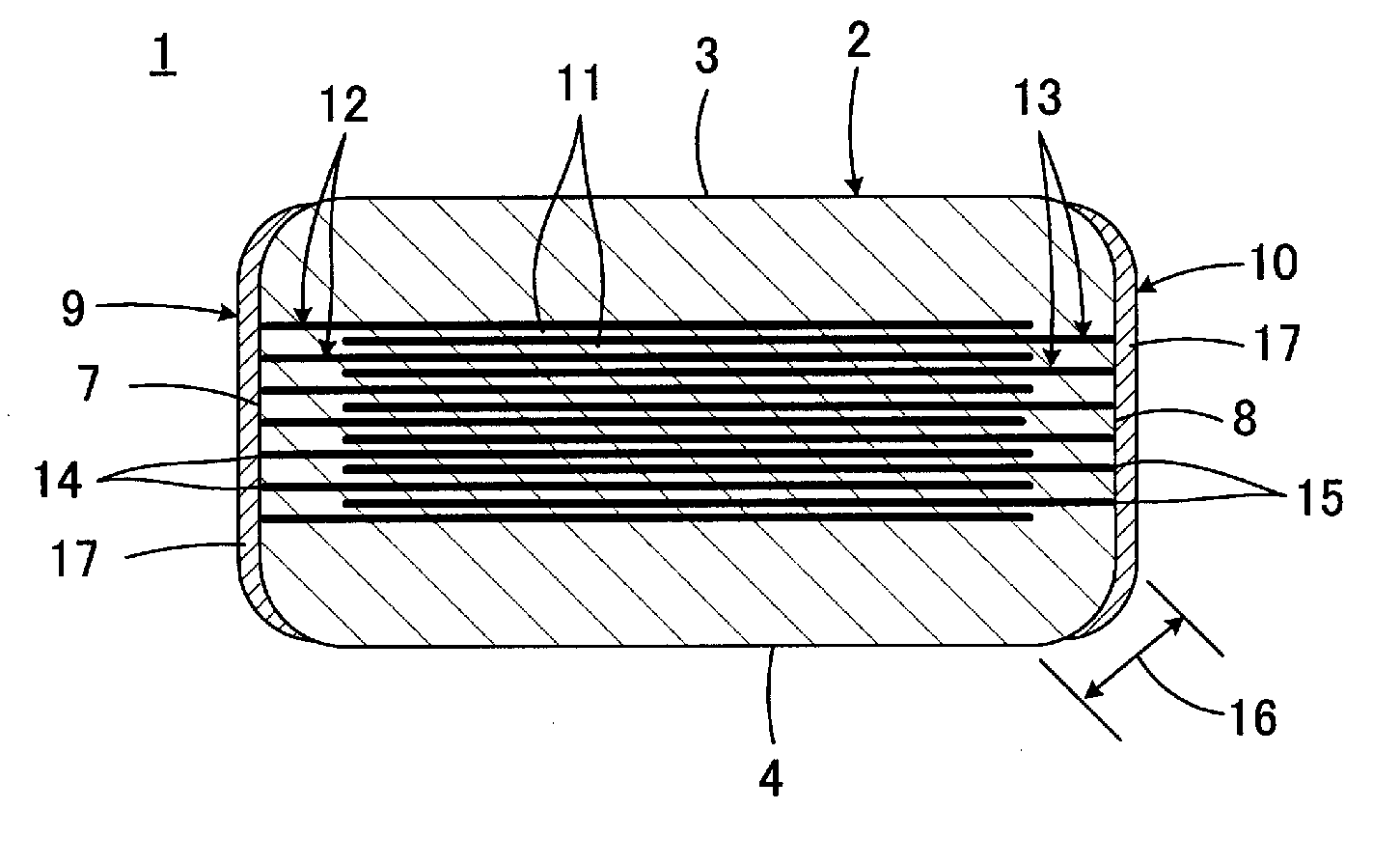
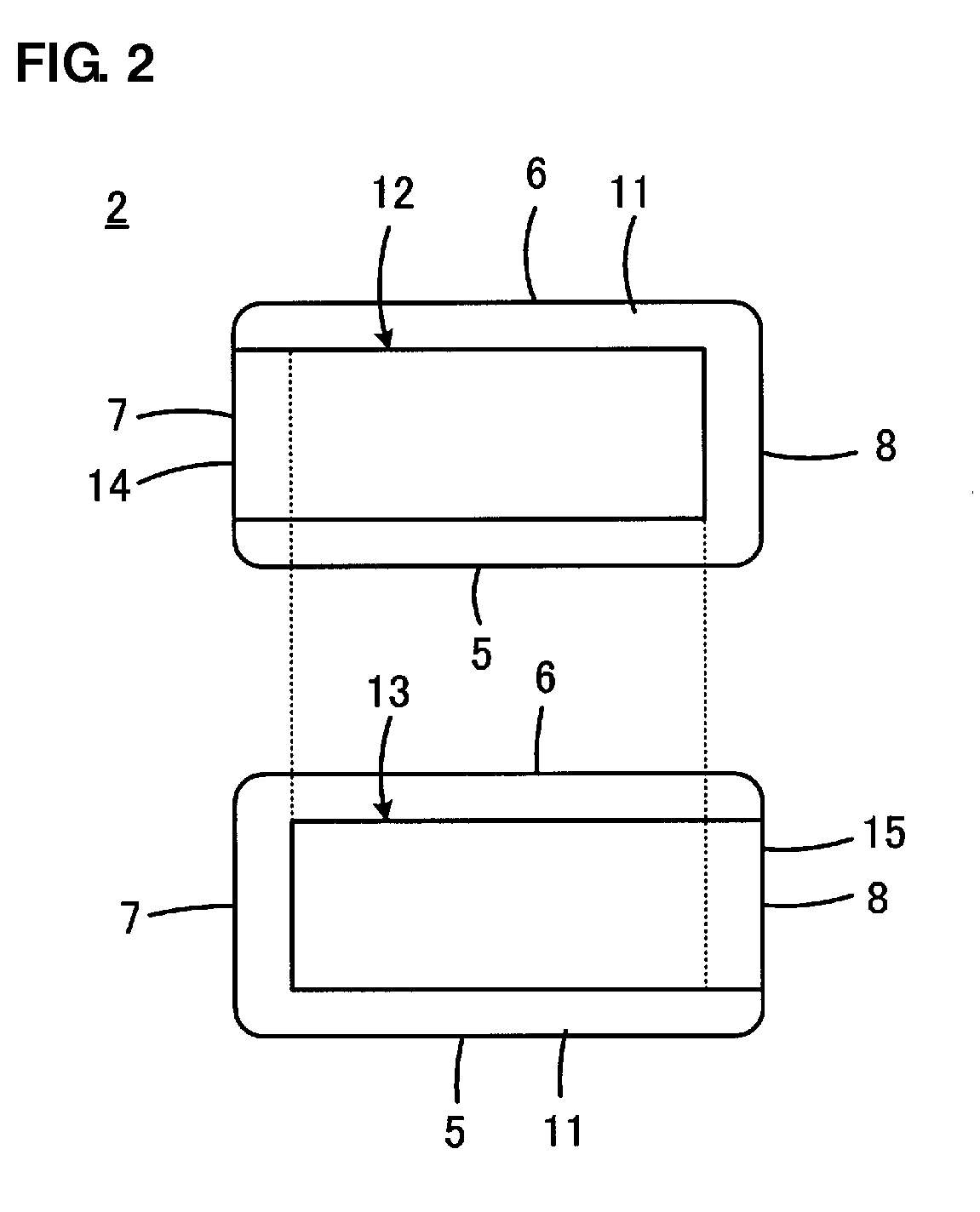
[0033]FIG. 1 is a cross-sectional view illustrating a laminated ceramic capacitor 1 as an example of a laminated ceramic electronic component according to a first preferred embodiment of the invention. The laminated ceramic capacitor 1 includes a ceramic element assembly 2. FIG. 2 is a plan view illustrating the internal structure of the ceramic element assembly 2.

[0034]Referring to FIGS. 1 and 2, the ceramic element assembly 2 preferably is a substantially rectangular parallelepiped shape having a pair of principal surfaces 3 and 4 facing each other, a pair of side surfaces 5 and 6 facing each other, and a pair of end surfaces 7 and 8 facing each other. On the first and second end surfaces 7 and 8 of the ceramic element assembly 2, first and second external terminal electrodes 9 and 10 are provided, respectively.

[0035]The ceramic element assembly 2 has a structure in which a plurality of ceramic layers 11 are laminated. In the ceramic element assembly 2, a plurality of pairs of fir...


PUM


Abstract

In a laminated ceramic electronic component, external terminal electrodes include plating films directly covering exposed portions of internal electrodes on end surfaces of a ceramic element assembly. On the boundaries between the end surfaces and principal surfaces of the ceramic element assembly, substantially rounded corners are provided, and the plating films are arranged such that the ends of the plating films stop at the corners and do not project from the principal surfaces.

Description

BACKGROUND OF THE INVENTION[0001]1. Field of the Invention[0002]The present invention relates to laminated ceramic electronic components, and particularly relates to the structure of external terminal electrodes to be provided on the laminated ceramic electronic components.[0003]2. Description of the Related Art[0004]In recent years, the market for compact portable electronic devices, such as cellular phones, notebook personal computers, digital cameras, and digital audio devices, has expanded. In the portable electronic devices, the size has been increasingly reduced and, simultaneously, the performance has been increasingly improved. A large number of laminated ceramic electronic components are mounted on portable electronic devices. There have demands on the laminated ceramic electronic components to reduce the size and improve the performance thereof. For example, it has been demanded of laminated ceramic capacitors to reduce the size and increase the capacitance.[0005]As a meas...

Claims


Application Information

Patent Timeline
IPC IPC(8): H01G4/228
CPCH01G4/232H01G4/30H01G4/2325
Inventor TAKEUCHI, SHUNSUKEKAWASAKI, KENICHIMOTOKI, AKIHIROOGAWA, MAKOTOIWANAGA, TOSHIYUKI
Owner MURATA MFG CO LTD
Why Eureka
Eureka Blog
Learn More