Apparatus for processing substrate and method of maintaining the apparatus

a technology for maintaining apparatus and substrate, applied in the direction of photomechanical apparatus, instruments, manufacturing tools, etc., can solve problems such as difficulty in maintenance work, and achieve the effect of reducing maintenance time and system downtime and improving production efficiency

Active Publication Date: 2010-05-20
SEMES CO LTD
View PDF12 Cites 5 Cited by
  • Summary
  • Abstract
  • Description
  • Claims
  • Application Information

AI Technical Summary

Benefits of technology

[0011]The present invention also provides a substrate processing system, in which a maintenance work can be easily performed to reduce maintenance time and system downtime and improve production efficiency.

Problems solved by technology

However, such a multi-stage structure makes it difficult to ensure a space necessary for repairing the inside of a processing apparatus, and thus it is difficult to perform a maintenance work.

Method used


Image

  • Apparatus for processing substrate and method of maintaining the apparatus
  • Apparatus for processing substrate and method of maintaining the apparatus
  • Apparatus for processing substrate and method of maintaining the apparatus

Examples


embodiment

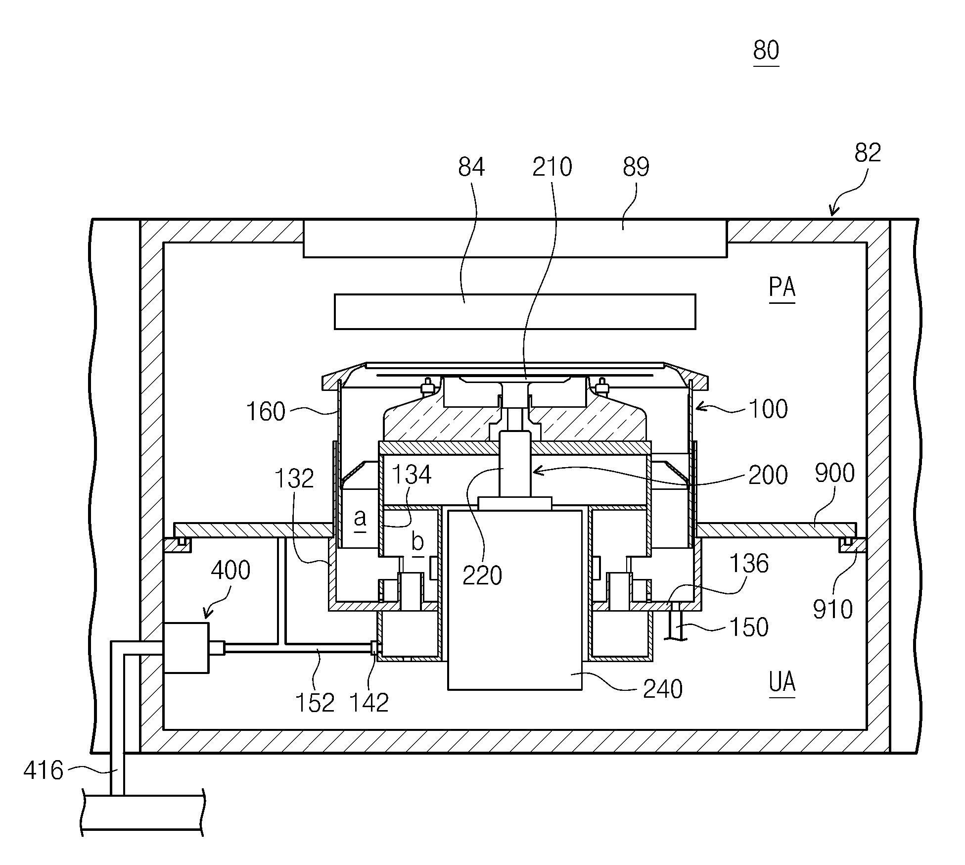
[0043]In the current embodiment, a semiconductor substrate is illustrated and explained as an example of substrates that can be processed using a substrate processing apparatus 1. However, the present invention is not limited thereto. That is, the present invention can be applied to various substrates such as a glass substrate.

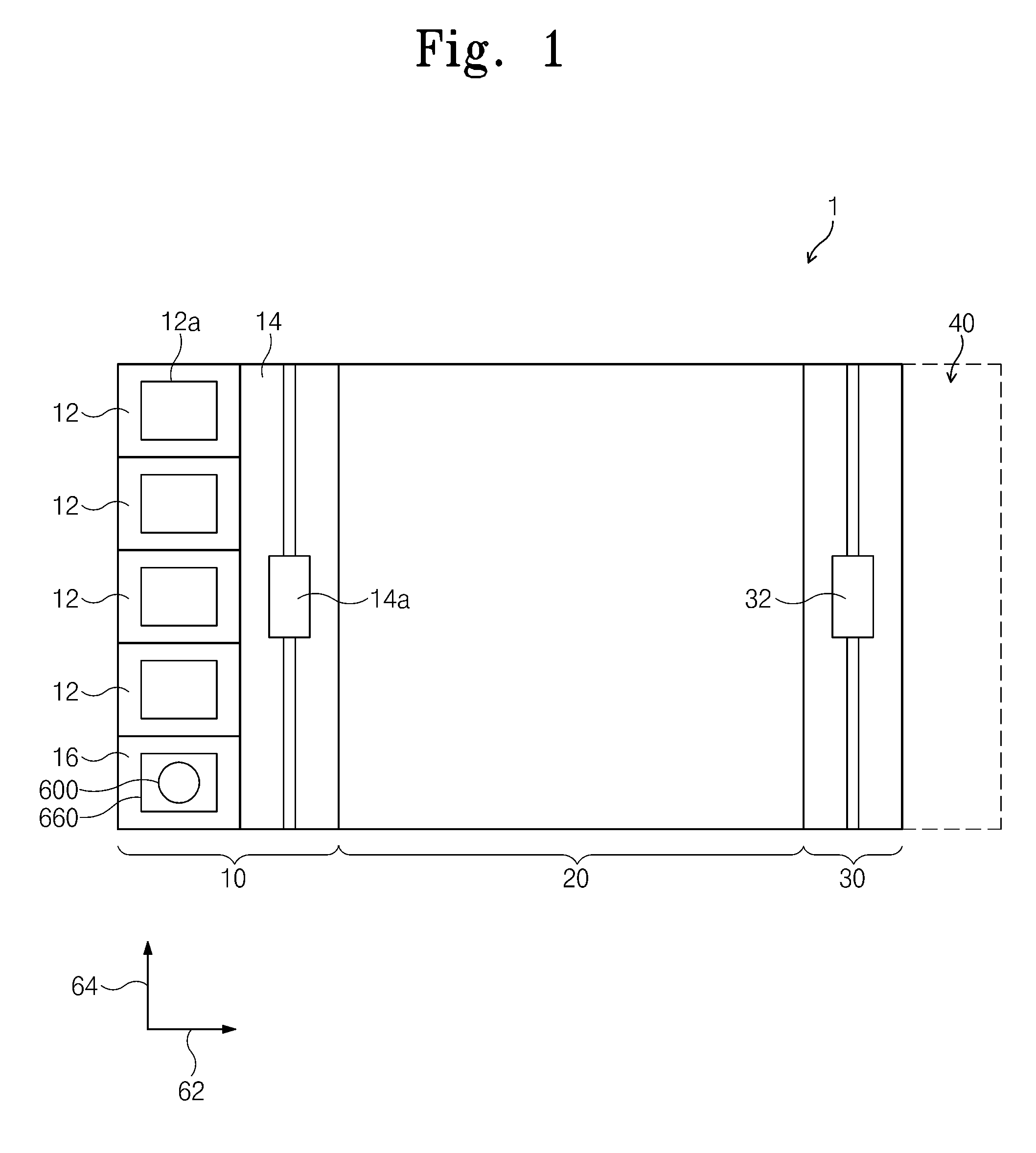
[0044]FIG. 1 is a schematic view illustrating a substrate processing apparatus 1 according to an embodiment of the present invention. The substrate processing apparatus 1 is used to perform a photolithography process on a wafer.

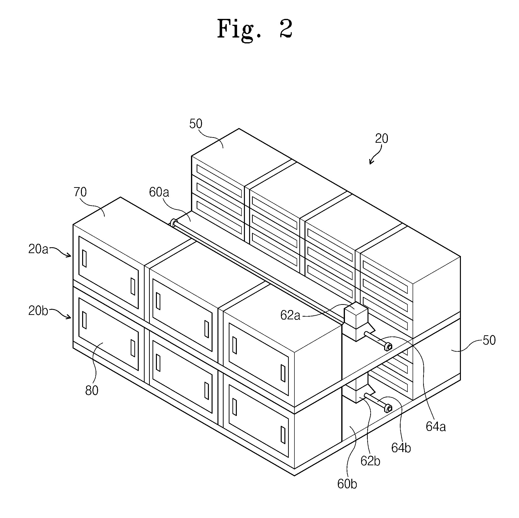
[0045]Referring to FIG. 1, the substrate processing apparatus 1 includes an index part 10, a process part 20, and an interface part 30, which are sequentially disposed in one direction (hereinafter, referred to as a first direction 62) in parallel with each other. The index part 10 includes cassette stages 12 and a robot passage 14.

[0046]Cassettes 12a in which semiconductor substrates such as wafers are accommodated are placed on the ca...


PUM

PropertyMeasurementUnit
lengthaaaaaaaaaa
electric characteristicsaaaaaaaaaa
temperatureaaaaaaaaaa

Abstract

Provided is an apparatus for processing a substrate. The apparatus includes a chamber, a process unit, and an exhaust member. The chamber has an inner space. The process unit is disposed at the inner space of the chamber and is movable outward from the chamber through a side of the chamber. The process unit includes an exhaust line. The exhaust member is disposed at the chamber. The exhaust member is connected to the exhaust line, and the exhaust member includes a movable exhaust port configured to be moved according to a movement of the process unit.

Description

CROSS-REFERENCE TO RELATED APPLICATIONS[0001]This U.S. non-provisional patent application claims priority under 35 U.S.C. §119 of Korean Patent Application No. 10-2008-0114532, filed on Nov. 18, 2008, the entire contents of which are hereby incorporated by reference.BACKGROUND OF THE INVENTION[0002]The present invention disclosed herein relates to an apparatus for processing a substrate and a method of maintaining the apparatus.[0003]Semiconductor devices are generally manufactured as follows: in a Fab process, electric circuits including electric devices are formed on a silicon wafer used as a semiconductor substrate; in an electrical die sorting (EDS) process, electric characteristics of semiconductor devices formed in the Fab process are inspected; and in a package assembly process, the semiconductor devices are respectively sealed with an epoxy resin and individually packaged.[0004]The Fab process includes sub processes such as a deposition process for forming a film on a wafer,...

Claims


Application Information

Patent Timeline
Patent Type & Authority Applications(United States)
IPC IPC(8): C23F1/00B23P19/00
CPCH01L21/6715H01L21/6719H01L21/68785H01L21/67051Y10T29/49815H01L21/67017G03F7/162G03F7/3021G03F7/70808H01L21/67703
Inventor NOH, HYOUNG-RAE
Owner SEMES CO LTD
Why Eureka
Try Eureka