

Lamb wave device
a technology of a beam wave and a resonant frequency, which is applied in the field of lamb wave devices, can solve the problem that the influence of film thickness variations on resonant frequency variations cannot become an ignorable level
- Summary
- Abstract
- Description
- Claims
- Application Information
AI Technical Summary
Benefits of technology
Problems solved by technology
Method used
Image

Examples
first embodiment
1 First Embodiment
1-1 Configuration of Lamb Wave Device 102
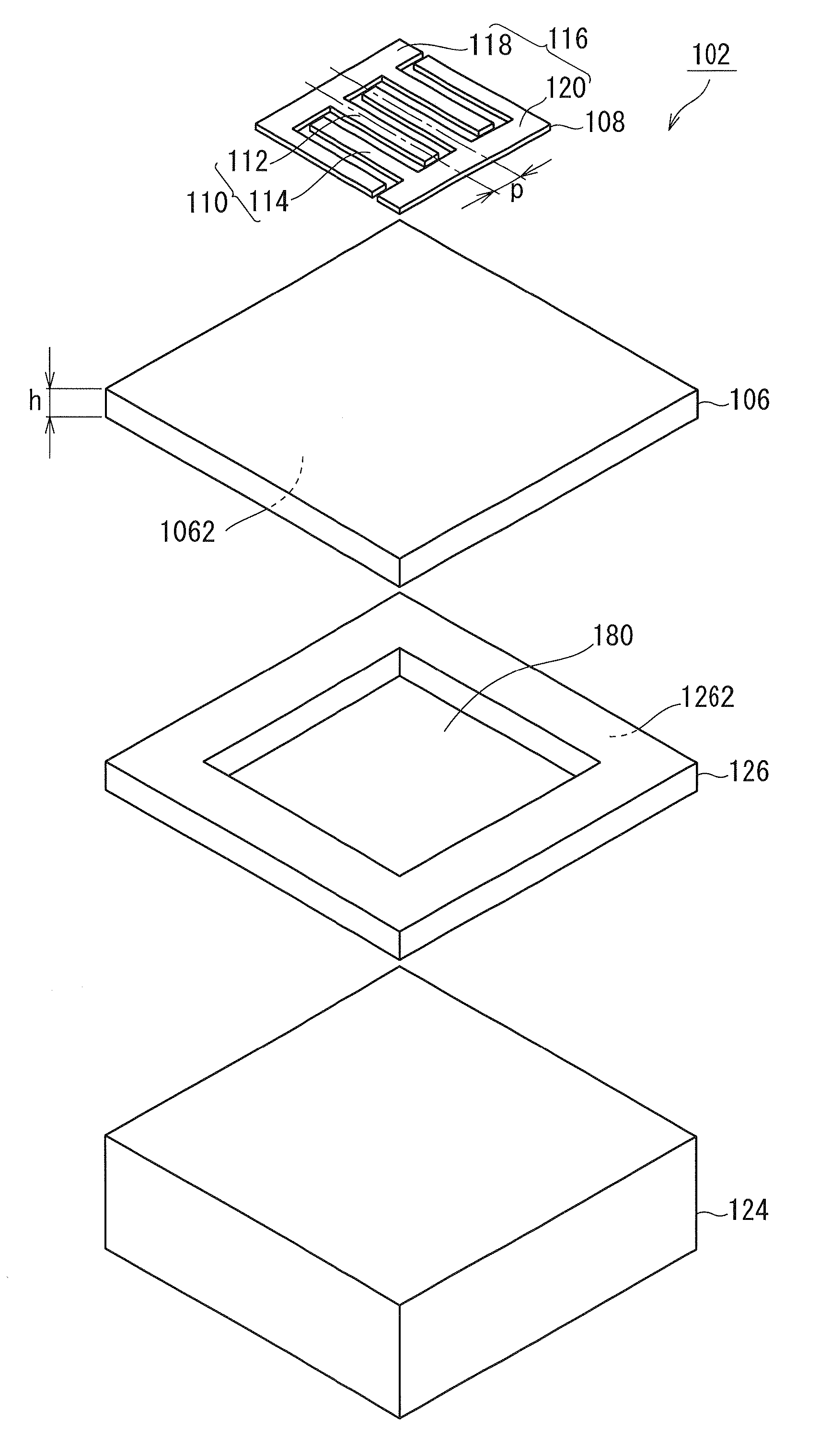
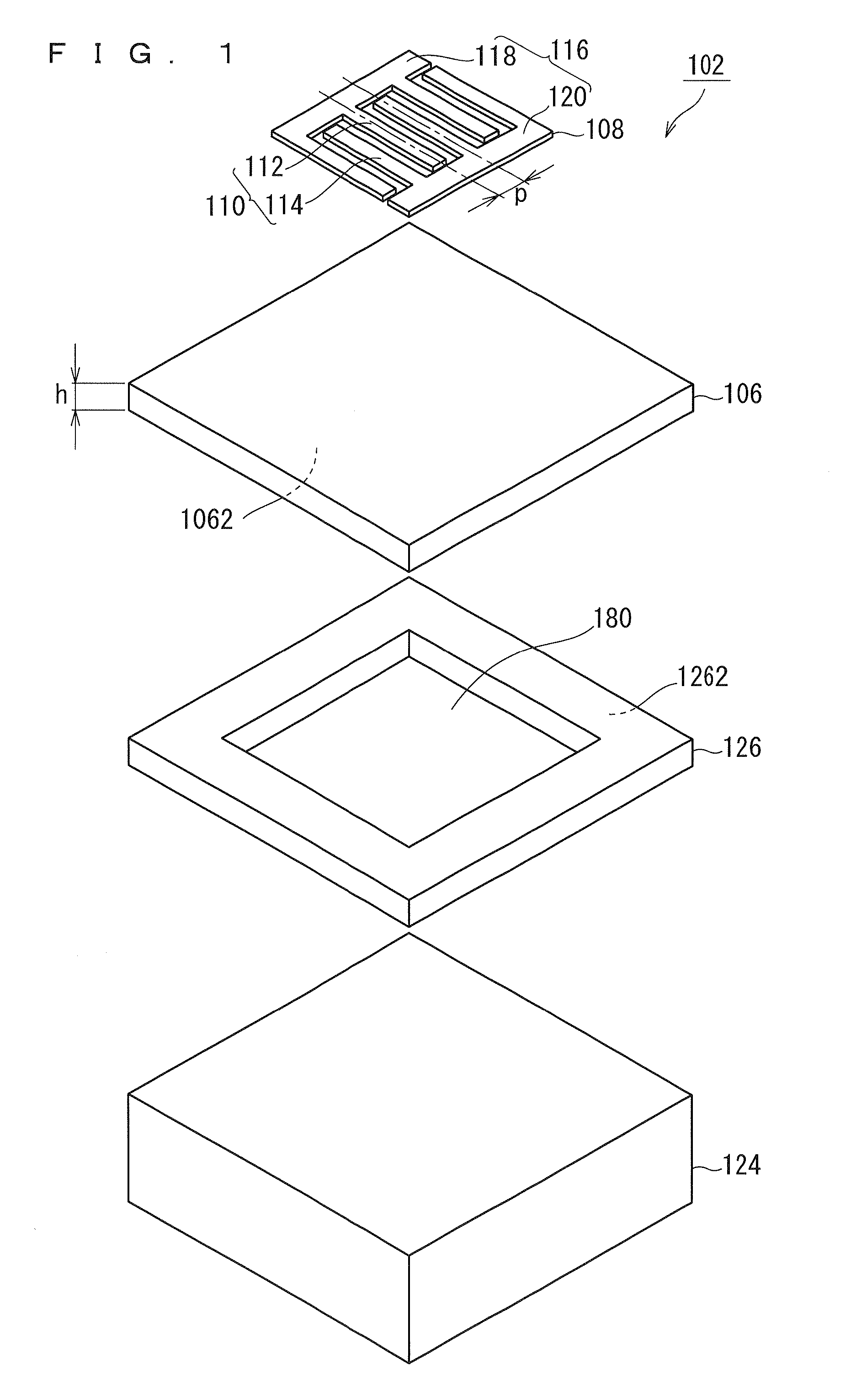
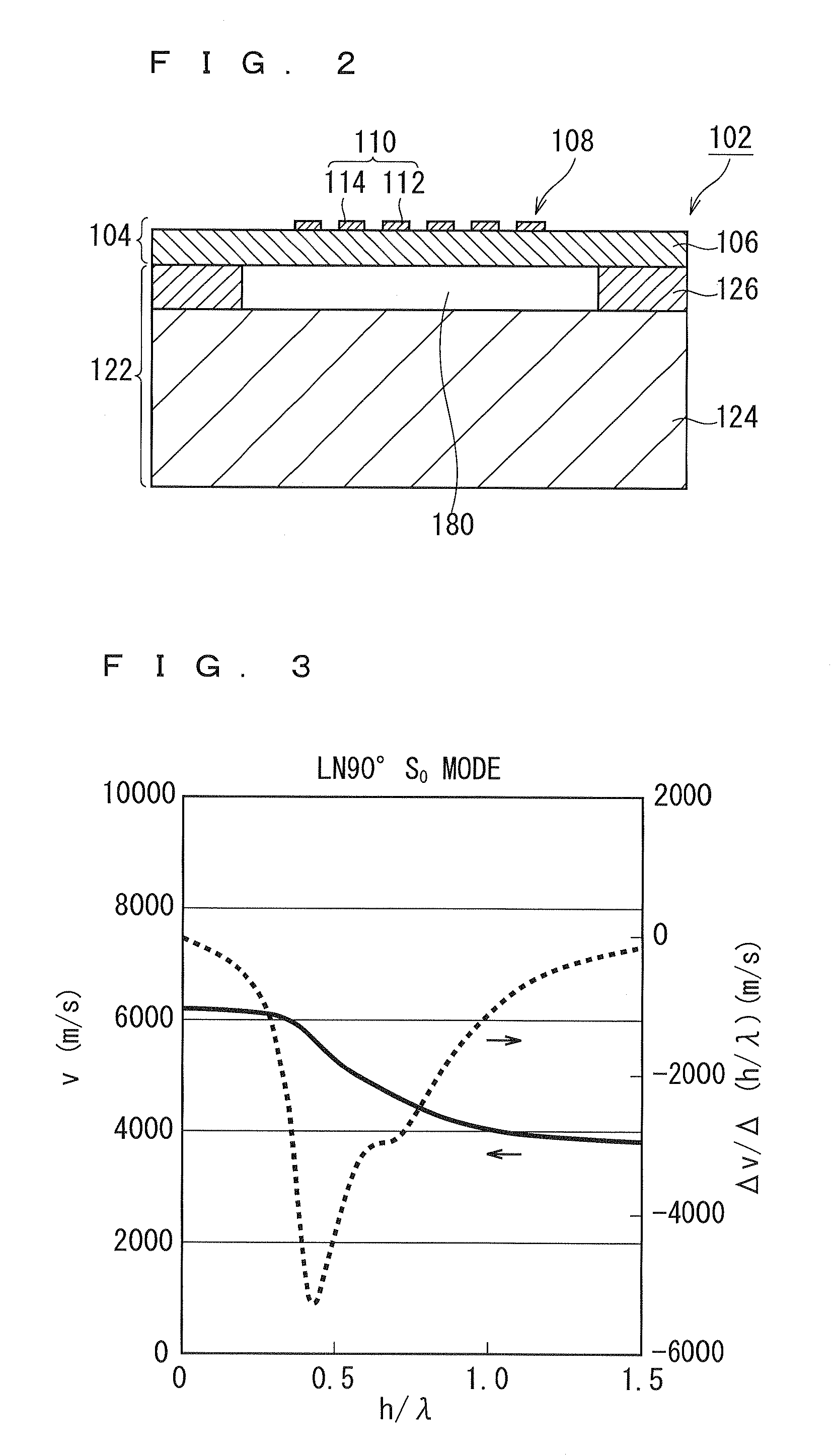
[0035]FIGS. 1 and 2 are schematic views of a lamb wave device 102 of a first embodiment. FIG. 1 is an exploded perspective view of the lamb wave device 102, and FIG. 2 is a sectional view of the lamb wave device 102.
[0036]As shown in FIGS. 1 and 2, the lamb wave device 102 has a structure in which a support structure 122 supports a laminate 104. The laminate 104 is provided with a piezoelectric thin film 106 and an. IDT electrode 108 that excites a lamb wave in the piezoelectric thin film 106. The support structure 122 is provided with a support substrate 124 and a support film 126 that bonds the support substrate 124 and the laminate 104. In the support film 126 formed is a cavity 180 that isolates an excitation section of the laminate 104 from the support substrate 124. The IDT electrode 108 is provided inside a region where the cavity 180 is formed (hereinafter referred to as a “cavity region”).
[0037]{Film Thickness h of ...
second embodiment
2 Second Embodiment
202>
[0071]A second embodiment relates to a lamb wave device 202 where, in place of the support structure 122 of the first embodiment, a support structure 222 supports a laminate 204 provided with a piezoelectric thin film 206 and an IDT electrode 208 in the same manner as in the first embodiment. FIG. 15 is a schematic view of the lamb wave device 202 of the second embodiment. FIG. 15 is a sectional view of the lamb wave device 202.
[0072]As shown in FIG. 15, the support structure 222 is provided with the support substrate 224, but is not provided with a support film. In the support substrate 224 formed is a cavity 280 for isolating an excitation section of the laminate 204 from the support substrate 224.
202>
[0073]FIGS. 16 to 18 are sectional views each explaining a manufacturing method for the lamb wave device 202. FIGS. 16 to 18 are sectional views of work-in-process products in the process of manufacturing.
[0074]{Production of Support Substrate 224}
[0075]In manu...
third embodiment
3 Third Embodiment
[0085]A third embodiment relates to a laminate 304 that can be adopted in place of the laminate 104 of the first embodiment, the laminate 204 of the second embodiment and a laminate 504 of a fifth embodiment. FIG. 19 is a schematic view of the laminate 304 of the third embodiment. FIG. 19 is a sectional view of the laminate 304.
[0086]As shown in FIG. 19, the laminate 304 is provided with an IDT electrode 309 in addition to a piezoelectric thin film 306 and an IDT electrode 308 which are similar to the piezoelectric thin film 106 and the IDT electrode 108 of the first embodiment. The IDT electrode 309 is provided on the under surface of the piezoelectric thin film 306. The IDT electrode 309 has a similar plane shape to the IDT electrode 308, and is provided in a position opposed to the IDT electrode 308. A finger 310 of the opposed IDT electrode 308 and a finger 311 of the IDT electrode 309 have the same phase.
[0087]Also in the case of adopting such IDT electrodes 3...
PUM
 Abstract
Description
Claims
Application Information