
Touch sensing substrate and touch sensing liquid crystal display

a liquid crystal display and touch sensing technology, applied in the field of touch sensing substrate and touch sensing liquid crystal display, can solve the problems of increasing the thickness of the added type touch sensing panel, unfavorable miniaturization, and just slightly less popular capacitive touch sensing panel than the resistive touch sensing panel, etc., to reduce the cross-talk

Active Publication Date: 2010-05-27
AU OPTRONICS CORP
View PDF6 Cites 45 Cited by
  • Summary
  • Abstract
  • Description
  • Claims
  • Application Information

AI Technical Summary

Benefits of technology

[0012]The present invention is directed to a touch sensing substrate capable of reducing cross-talk effect between a common electrode and sensing series.
[0013]The present invention is further directed to a touch sensing LCD having dummy sensing series for reducing erroneous actions.
[0020]According to an embodiment of the present invention, resistance of the bridge lines is lower than resistance of the sensing pads.
[0031]According to an embodiment of the present invention, resistance of the bridge lines is lower than resistance of the sensing pads.
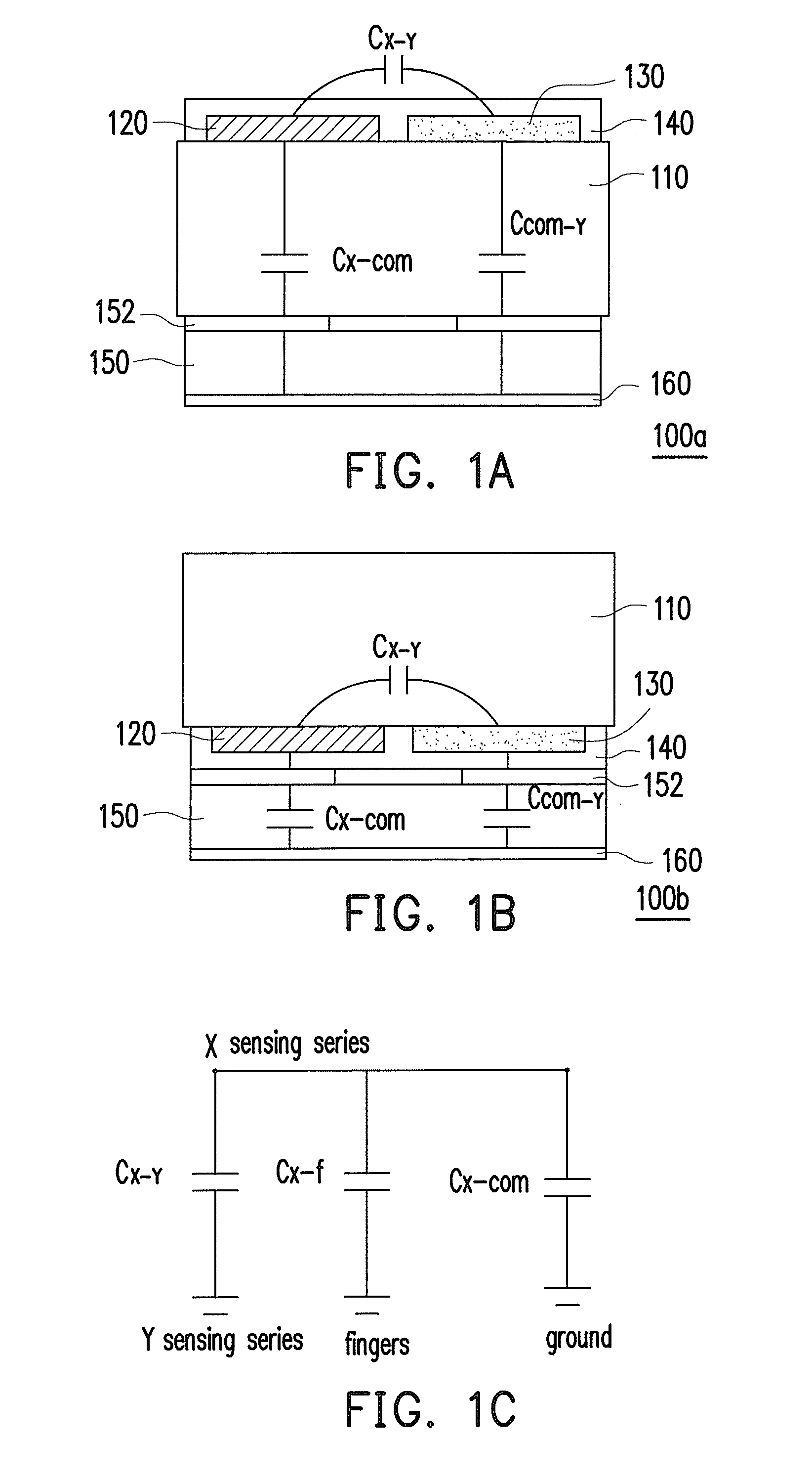
[0036]Since the dummy sensing series of the present invention reduce the cross-talk effect between the common electrode and the sensing series, sensitivity of the touch sensing substrate is not apt to decrease notwithstanding interferences of the parasitical capacitance.

Problems solved by technology

Therefore, the capacitive touch sensing panel is just slightly less popular than the resistive touch sensing panel.
Apparently, the substrate of the added type touch sensing panel brings about an increase in entire thickness of the added type touch sensing panel, which is unfavorable to miniaturization and microminiaturization of the display.

Method used


Image

  • Touch sensing substrate and touch sensing liquid crystal display
  • Touch sensing substrate and touch sensing liquid crystal display
  • Touch sensing substrate and touch sensing liquid crystal display

Examples


Embodiment Construction

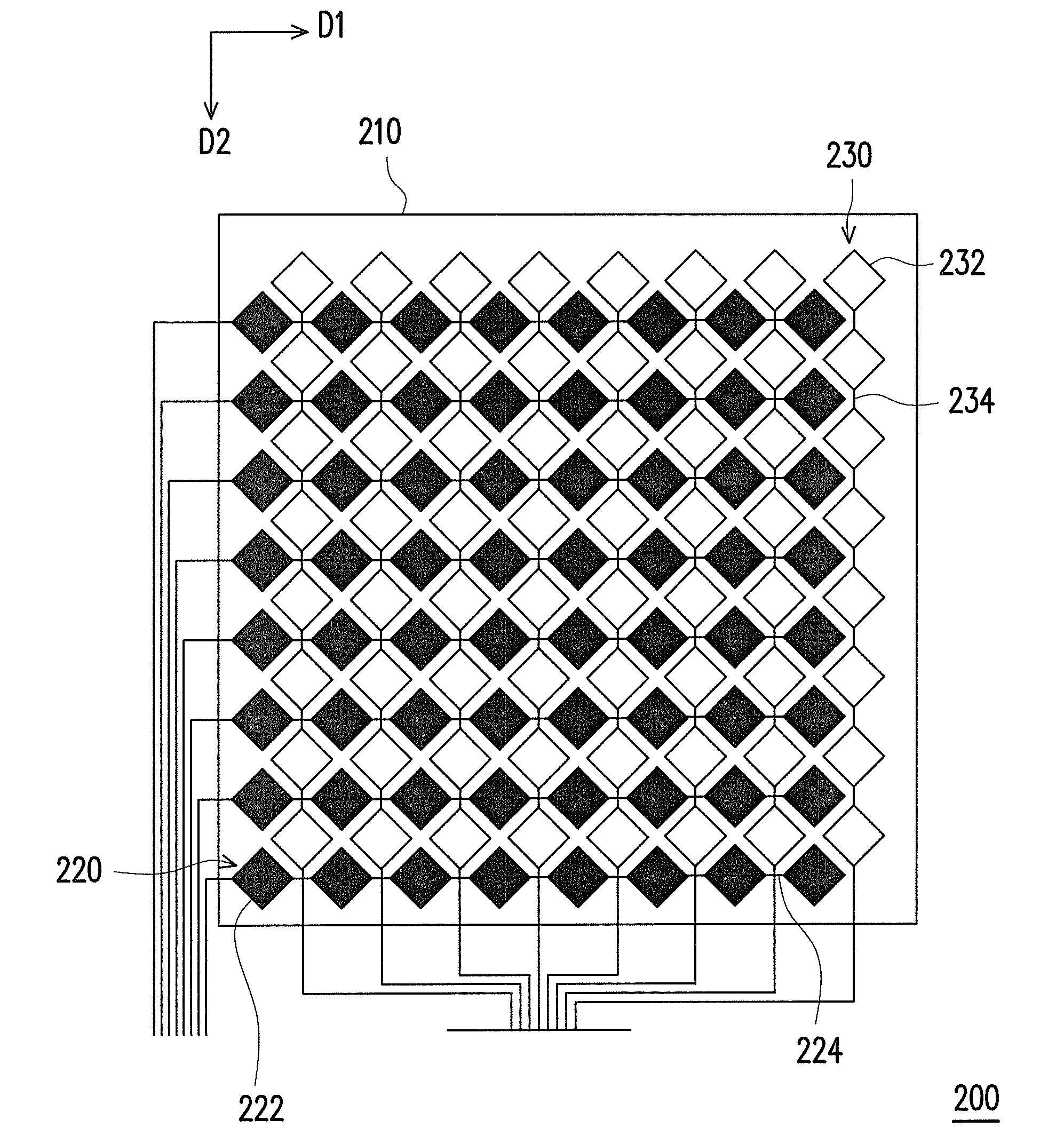
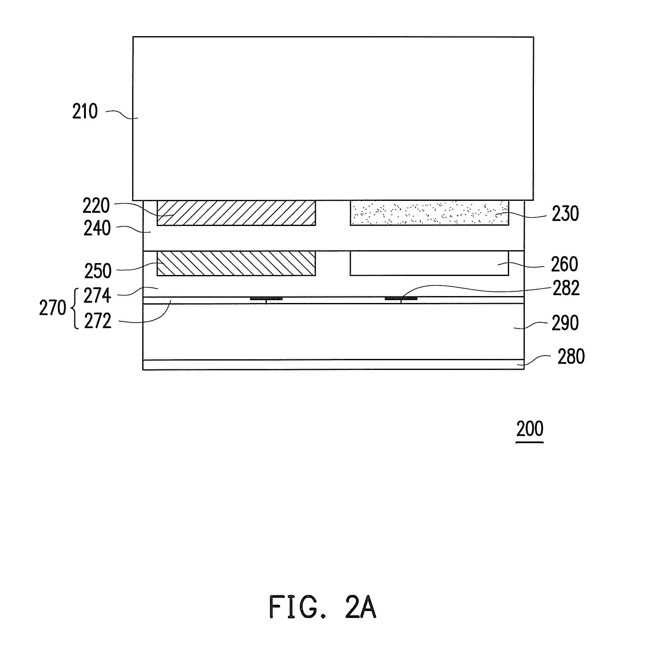
[0047]FIG. 2A is a schematic view of a touch sensing substrate according to an embodiment of the present invention. Referring to FIG. 2A, a touch sensing substrate 200 of the present embodiment includes a substrate 210, a plurality of first sensing series 220, a plurality of second sensing series 230, a first dielectric layer 240, a plurality of first dummy sensing series 250, a plurality of second dummy sensing series 260, a second dielectric layer 270, and a common electrode 280. The first sensing series 220 (e.g. X sensing series) are electrically insulated from each other, and so are the second sensing series 230 (e.g. Y sensing series). The first dielectric layer 240 covers the first sensing series 220 and the second sensing series 230. The first dummy sensing series 250 are disposed on the first dielectric layer 240 and located above the first sensing series 220. Note that the first dummy sensing series 250 are electrically insulated from each other, and each of the first dumm...


PUM


Abstract

A touch sensing substrate includes a substrate, first and second sensing series, a first dielectric layer, first and second dummy sensing series, a second dielectric layer, and a common electrode. The first sensing series are electrically insulated from each other, and so are the second sensing series. The first and the second sensing series are covered by the first dielectric layer. The first and the second dummy sensing series are disposed on the first dielectric layer. The first and the second dummy sensing series are disposed above the first and the second sensing series, respectively, and the dummy sensing series and the sensing series corresponding thereto have the same potential. The first and the second dummy sensing series are covered by the second dielectric layer. The common electrode is disposed on the second dielectric layer. A touch sensing liquid crystal display having the above-mentioned touch sensing substrate is also provided.

Description

CROSS-REFERENCE TO RELATED APPLICATION[0001]This application claims the priority benefit of Taiwan application serial no. 97145558, filed on Nov. 25, 2008. The entirety of the above-mentioned patent application is hereby incorporated by reference herein and made a part of specification.BACKGROUND OF THE INVENTION[0002]1. Field of the Invention[0003]The present invention relates to a touch sensing substrate and a touch sensing liquid crystal display (LCD). More particularly, the present invention relates to a low noise touch sensing substrate and a low noise touch sensing LCD.[0004]2. Description of Related Art[0005]Based on different sensing types, a touch sensing panel can be generally categorized into a resistive touch sensing panel, a capacitive touch sensing panel, an optical touch sensing panel, an acoustic-wave touch sensing panel, and an electromagnetic touch sensing panel. The capacitive touch sensing panel is characterized by short response speed, favorable reliability, sat...

Claims


Application Information

Patent Timeline
IPC IPC(8): G06F3/045G06F3/041
CPCG06F3/044G06F3/0445
Inventor LO, CHENGCHENG, CHING-SHENGLIN, YUNG-LUNHU, CHIH-JEN
Owner AU OPTRONICS CORP
Learn More