Package-on-package device, semiconductor package and method for manufacturing the same

US20100133675A1Active Publication Date: 2010-06-03ADVANCED SEMICON ENG INC
5 Cites 113 Cited by

Patent Information

Authority / Receiving Office
US · United States
Patent Type
Applications(United States)
Current Assignee / Owner
Publication Date
2010-06-03

Smart Images

  • Figure 1
    Figure 1
  • Figure 2
    Figure 2
  • Figure 3
    Figure 3
Patent Text Reader

Abstract

A semiconductor package includes a substrate, a chip, an interposer and a molding compound. The chip is electrically connected to the upper surface of the substrate. The interposer is disposed on the chip, and electrically connected to the upper surface of the substrate. The interposer includes an embedded component and a plurality of electric contacts, wherein the embedded component is located between the upper and lower surfaces of the interposer, and the electric contacts are located on the upper surface of the interposer. The molding compound seals the chip and covers the upper surface of the substrate and the lower surface of the interposer.
Need to check novelty before this filing date? Find Prior Art

Description

CROSS REFERENCE TO RELATED APPLICATION

[0001] This application claims the priority benefit of Taiwan Patent Application Serial Number 097146551, filed on Dec. 1, 2008, the full disclosure of which is incorporated herein by reference.BACKGROUND OF THE INVENTION

[0002] 1. Field of the Invention

[0003] The present invention generally relates to a stacked package device, and more particularly to a bottom package of a stacked package device including an interposer.

[0004] 2. Description of the Related Art

[0005] Currently, a package-on-package (hereinafter referred to as POP) device is related to a semiconductor package disposed on another semiconductor package. The basic object of the POP device is to increase the density of components so as to result in more functions of components per unit volume and better regional efficiency. Thus, the total area of the POP device can be decreased, and the cost is reduced simultaneously.

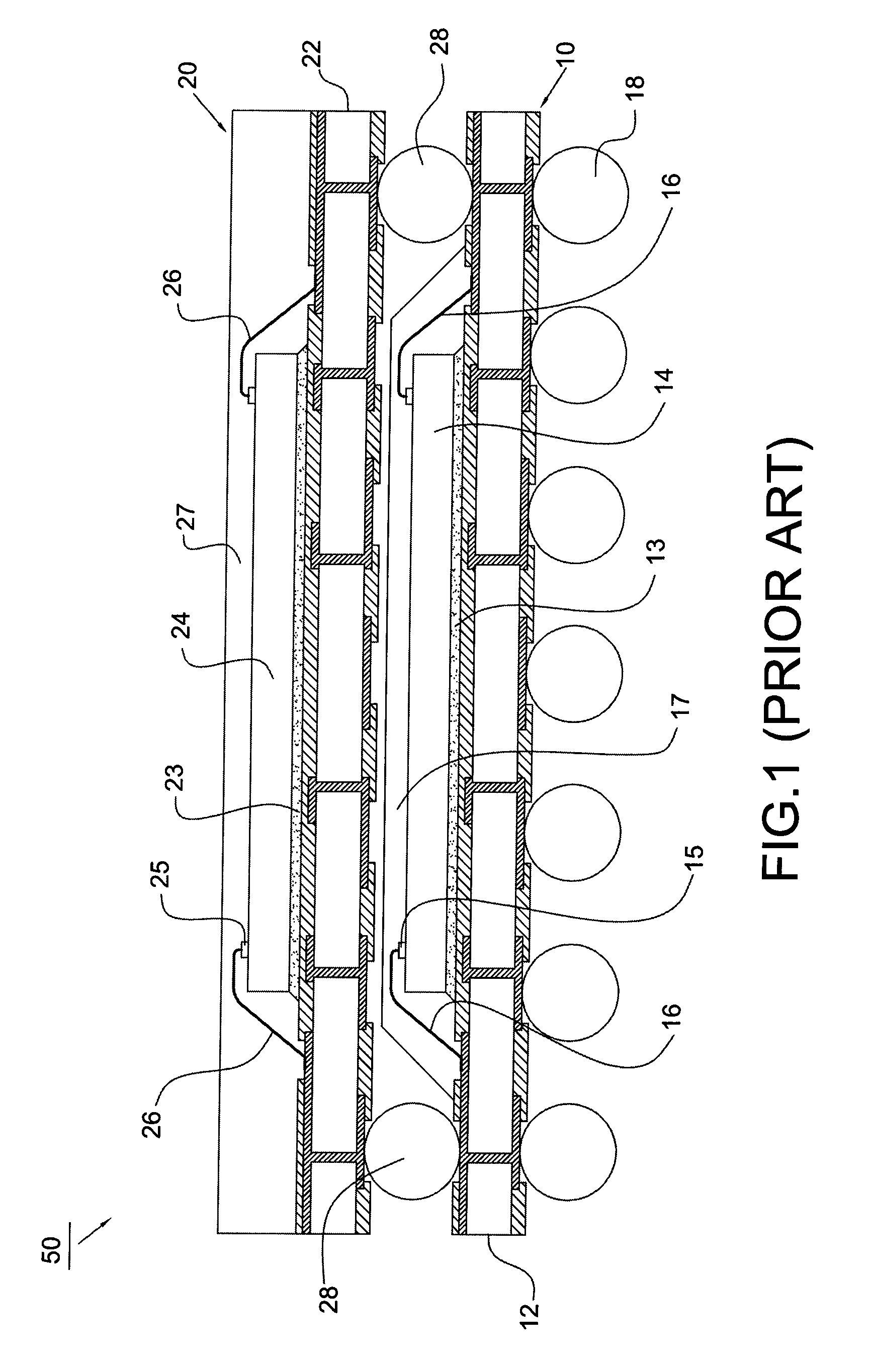
[0006] FIG. 1 is a diagrammatic sketch in a sectional view illustrating th...

Examples

Embodiment Construction

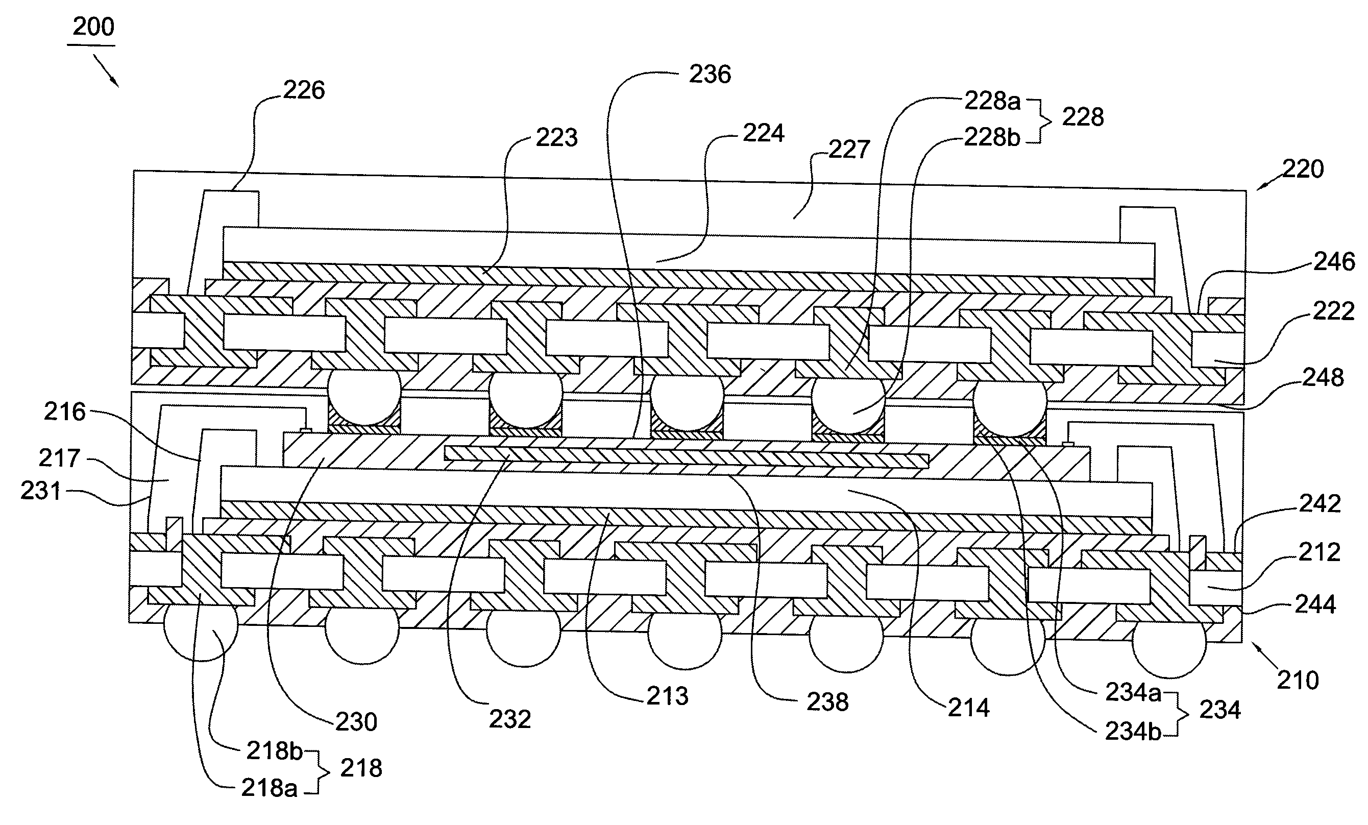
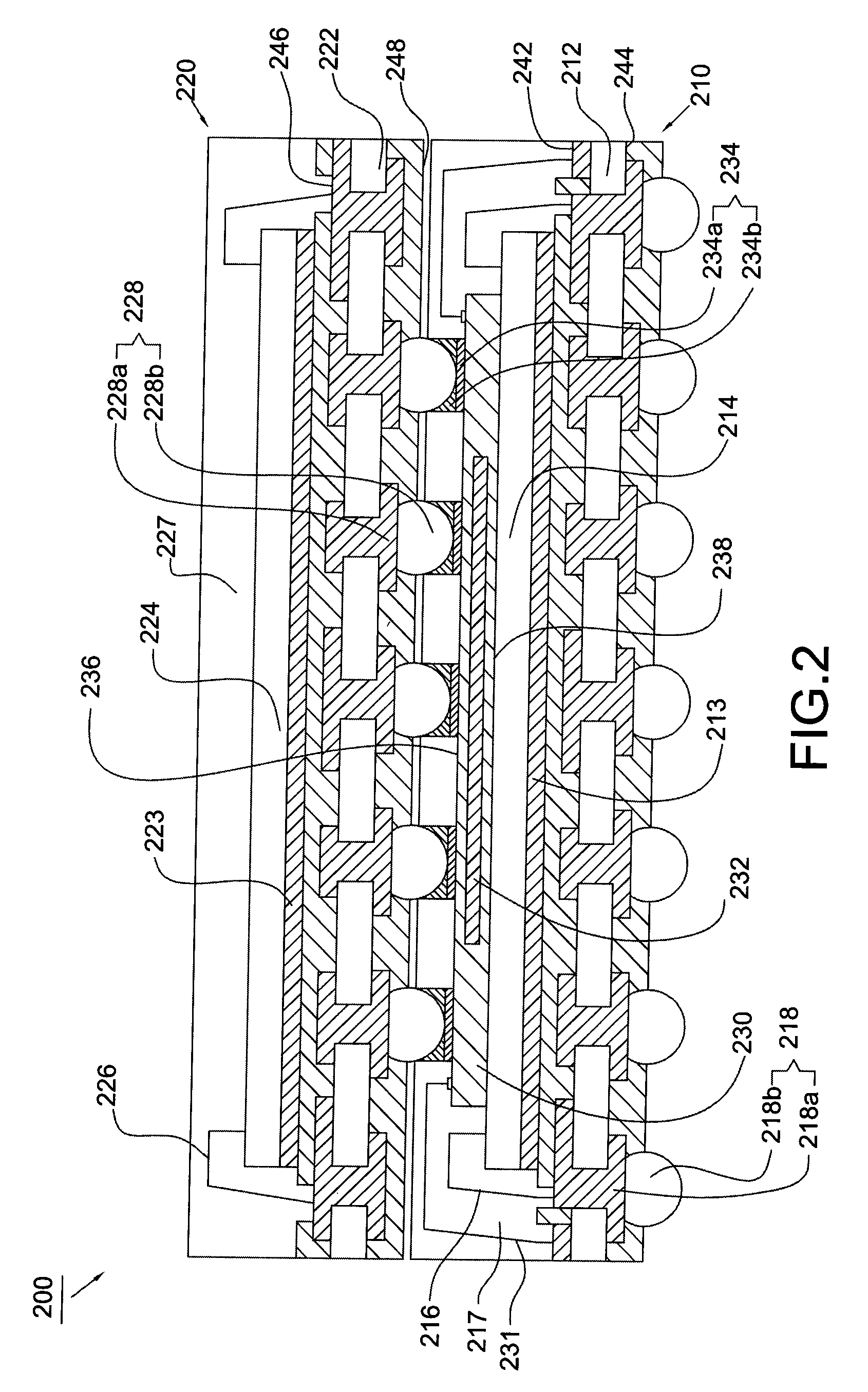
[0019]Referring to FIG. 2, it depicts a stacked package (i.e. package-on-package, POP) device 200 according to an embodiment of the present invention. The POP device 200 includes a top package 220 and a bottom package 210.

[0020]The bottom package 210 includes a first chip 214 mounted and electrically connected to an upper surface 242 of a first substrate 212. The first substrate 212 of the bottom package 210 has upper and lower metal layers which can be patterned to provide appropriate circuitry and electrically connected by way of vias. An interposer 230 is disposed on the first chip 214 and electrically connected to the upper surface 242 of the first substrate 212. Referring to FIG. 3, the interposer 230 can be a multi-layer circuit substrate or a silicon substrate with circuit formed therein. For example, a silicon substrate 130 has an upper surface 136 and a lower surface 138. An embedded component 232 is disposed within an opening 132 of the silicon substrate 130 and secured by...