A power semiconductor arrangement and a semiconductor valve provided therewith

a technology of power semiconductor and semiconductor valve, which is applied in the direction of semiconductor devices, semiconductor/solid-state device details, electrical apparatus, etc., can solve the problems that the solution according to prior art seems less effective in adopting deviations, and achieve the effect of transforming and effective adoption

Inactive Publication Date: 2010-06-03
ABB TECH AG
View PDF5 Cites 13 Cited by
  • Summary
  • Abstract
  • Description
  • Claims
  • Application Information

AI Technical Summary

Benefits of technology

[0015]The object of the invention is achieved by the initially defined power semiconductor arrangement, characterised in that said at least one support surface of said at least one spring element is laterally stationary arranged in relation to said at least one corresponding support surface upon compression motion of said spring element. Accordingly, there will be no lateral sliding motion between the at least one spring element and any of its neighbouring elements against which it bears. As a result thereof, friction forces that would counteract a correct adoption of non-parallelism by means of the spring element(s) are avoided, and a more uniform pressure distribution than otherwise is achieved. This is an essential difference to prior art as mentioned earlier, which, for the adoption of non-parallelism, relies on movements between individual parts (ball and ball-seat, spring element and adjacent surface) that are of sliding, and therefore friction-loss inducing, character. The technical effect of the invention will increase along with increasing clamping forces. It should be noted that said compression motion of the spring element includes uneven compression of the spring element, by which one side of the spring element becomes more compressed than another side thereof.
[0016]According to one embodiment, said at least one spring element is arranged between said first clamping element and said power semiconductor element, and where the adjacent element is said first clamping element.
[0017]According to one embodiment, the power semiconductor arrangement comprises a third clamping element, which is arranged between said spring element and said at least one power semiconductor element, wherein the adjacent element of said spring element is said third clamping element.
[0018]According to one embodiment, said third clamping element is tiltable in relation to said first clamping element through the action of said spring element.
[0019]According to one embodiment, said at least one spring element comprises a helical spring. A helical spring has the advantage of being able to adopt deviations from parallelism between elements on opposite sides thereof, and upon compression thereof, without any sliding, friction-force inducing motion being necessitated between the contact surfaces of the spring and said further elements.
[0020]According to one embodiment, the power semiconductor arrangement comprises a plurality of spring elements arranged in parallel with each other. The arrangement of a plurality of spring elements may be advantageous from a fail-safe point of view, but also adds to a more versatile and effective adoption of deviations from parallelism between elements on opposite thereof.

Problems solved by technology

However, at higher clamping forces, the solutions according to prior art seems to be less effective in adopting deviations in parallelism and, thereby, guaranteeing a uniform pressure distribution on contact surfaces between the power semiconductor elements and their neighbouring elements.

Method used


Image

  • A power semiconductor arrangement and a semiconductor valve provided therewith
  • A power semiconductor arrangement and a semiconductor valve provided therewith
  • A power semiconductor arrangement and a semiconductor valve provided therewith

Examples


Embodiment Construction

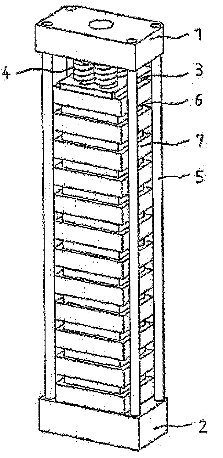
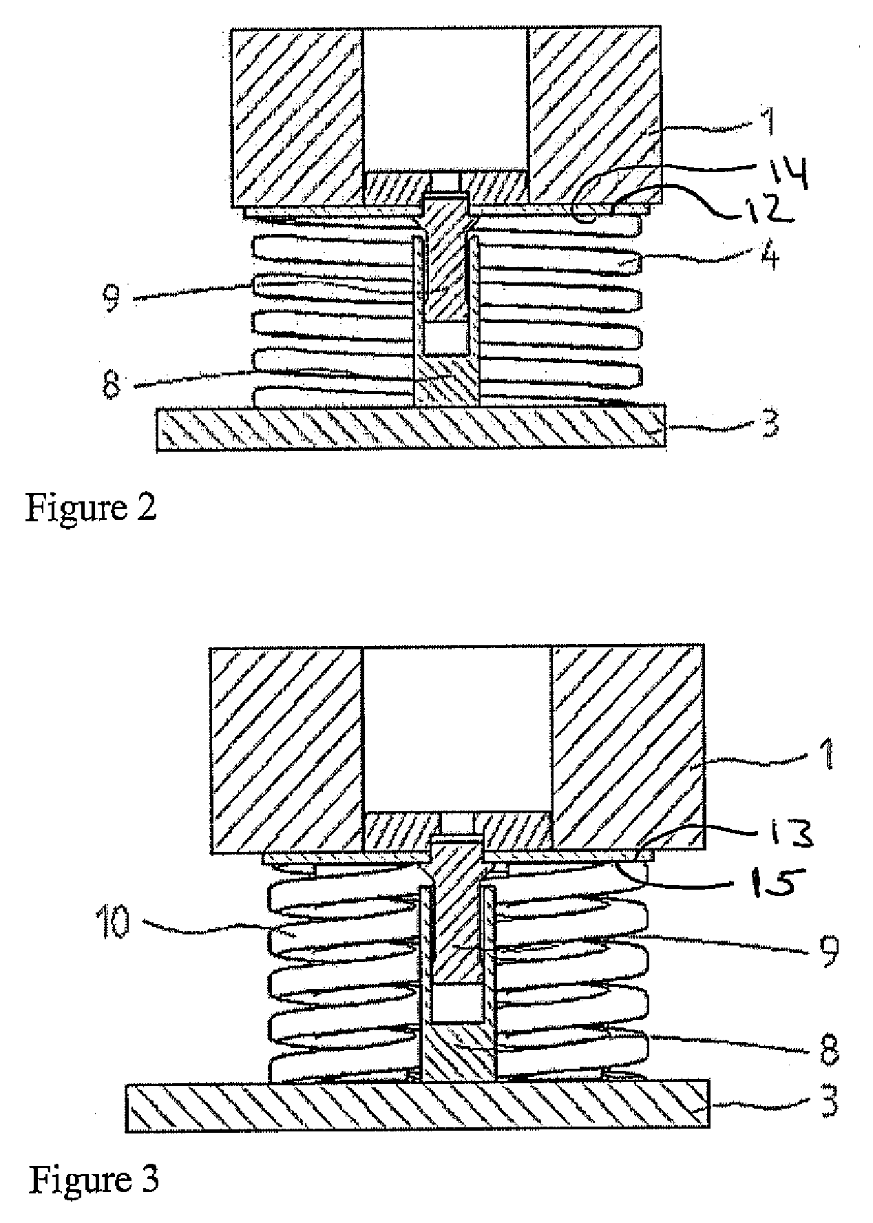
[0036]FIG. 1 shows a first embodiment of a power semiconductor arrangement according to the invention. Preferably, the arrangement forms a module in a thyristor, for example a so called IGBT, or transistor in which, typically, high voltage direct current is converted to alternating current or in which high voltage alternating current is converted to direct current.

[0037]The arrangement comprises a clamping device that comprises a first clamping element 1, a second clamping element 2, a third clamping element 3, and a plurality of spring elements 4 arranged between the first clamping element 1 and the third clamping element 3. The clamping device also comprises a frame structure, in this case a plurality of elongated members 5 such as rods, that extends between and interconnects the first clamping element 1 to the second clamping element 2.

[0038]Between the first clamping element 1 and the third clamping element 2 there is provided a plurality of power semiconductor elements 6 and a ...


PUM


Abstract

A power semiconductor arrangement including a clamping device including a first clamping element and a second clamping element. A plurality of power semiconductor elements are stacked on each other between the first and second clamping elements of the clamping device. The first clamping element receives a clamping force in an axial direction of the stack of the power semiconductor elements. At least one spring element is arranged between the first clamping element and the power semiconductor elements. The at least one spring element presents at least one support surface with which the at least one spring element bears against at least one corresponding support surface of an adjacent element. The at least one spring element includes a helical spring. A center axis of the at least one spring element coincides with a center of the clamping force, or the at least one spring element includes a plurality of helical springs arranged in parallel with each other, which are arranged symmetrically in relation to a point in which a center of the clamping force is introduced into the first clamping element.

Description

TECHNICAL FIELD[0001]The present invention relates to a power semiconductor arrangement, comprising: at least one power semiconductor element; a clamping device, comprising a first clamping element and a second clamping element, said power semiconductor element being arranged between said first and second clamping elements; and at least one spring element arranged between said first clamping element and said power semiconductor element, wherein said at least one spring element presents at least one support surface with which it bears against at least one corresponding support surface of an adjacent element.[0002]The invention also relates to a semiconductor valve, such as the ones used in thyristors or Insulated Gate Bipolar Transistors (IGBTs) or Integrated Gate Commutated Thyristors (IGCTs), provided with a power semiconductor arrangement according to the invention.[0003]A power semiconductor element is referred to as an element that turn high current on and off at high voltage le...

Claims


Application Information

Patent Timeline
Patent Type & Authority Applications(United States)
IPC IPC(8): H01L25/065H01L21/70H01L23/52
CPCH01L24/72H01L25/117H01L2924/01002H01L2924/01015H01L2924/01033H01L2924/13055H01L2924/19043H01L2924/1305H01L2924/1301H01L2924/01023H01L2924/00
Inventor SANDIN, BJORN
Owner ABB TECH AG
Why Eureka
Try Eureka