Inner and outer layer copper thickness-differentiated thick copper circuit board and preparation method thereof

A technology of thick copper circuit boards, inner and outer layers, applied in multilayer circuit manufacturing, printed circuit manufacturing, removal of conductive materials by chemical/electrolytic methods, etc. It can achieve the effect of good filling effect, no bubbles in lamination, and improvement of hole quality problems.

Active Publication Date: 2015-04-01
KALEX MULTI LAYER CIRCUIT BOARD (ZHONGSHAN) CO LTD
View PDF4 Cites 14 Cited by
  • Summary
  • Abstract
  • Description
  • Claims
  • Application Information

AI Technical Summary

Problems solved by technology

[0004] However, when the 12OZ thick copper plate is stacked on the inner layer, there is a large space to be filled with resin between the lines, and the circuit board is an outer layer of 6OZ inner layer of 12OZ thick copper plate, which has a large thickness and obvious barrier effect, which is not conducive to filling. Many, uneven heat transfer, prone to problems such as air bubbles and poor pressing

Method used


Image

  • Inner and outer layer copper thickness-differentiated thick copper circuit board and preparation method thereof
  • Inner and outer layer copper thickness-differentiated thick copper circuit board and preparation method thereof
  • Inner and outer layer copper thickness-differentiated thick copper circuit board and preparation method thereof

Examples


Embodiment 1

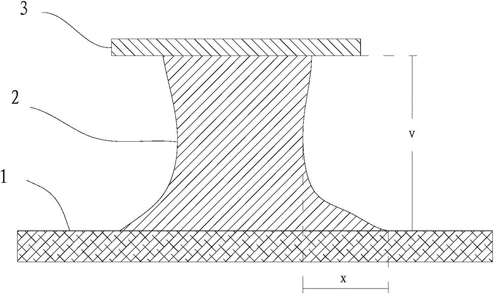
[0064] A method for preparing a thick copper circuit board (inner layer 12OZ, outer layer 6OZ thick copper board) with inconsistent copper thicknesses on the inner and outer layers, the circuit board adopts a four-layer structure, wherein the first and fourth circuit layers use 6OZ thick copper foil 12OZ thick copper foil is used for the second and third circuit layers, and the board thickness is 65-81mil.

[0065] The preparation method of this embodiment includes the steps of plate pressing, drilling and etching, and the other steps are prepared according to conventional methods. in:

[0066] (1) In the pressing process, the 1080 prepreg with a resin content of 68% is selected, and the hot pressing process and the cold pressing process are used for pressing in turn; the specific process parameters are shown in the table below.

[0067] Table 1. Setting of pressing plate process parameters

[0068]

[0069]

[0070] In the above-mentioned cold pressing process, the co...

Embodiment 2

[0077] A method for preparing a thick copper circuit board (inner layer 12OZ, outer layer 6OZ thick copper board) with inconsistent copper thicknesses on the inner and outer layers, the circuit board adopts a four-layer structure, wherein the first and fourth circuit layers use 6OZ thick copper foil 12OZ thick copper foil is used for the second and third circuit layers, and the board thickness is 65-81mil.

[0078] The preparation method of this embodiment includes the steps of plate pressing, drilling and etching, and the other steps are prepared according to conventional methods. in:

[0079] (1) In the pressing process, the 1080 prepreg with a resin content of 71% is selected, and the hot pressing process and the cold pressing process are used for pressing in turn; the specific process parameters are shown in the table below.

[0080] Table 3. Setting of pressing plate process parameters

[0081]

[0082] (2) In the drilling process, the board is baked at 120°C for 6 h...

Embodiment 3

[0088] A method for preparing a thick copper circuit board (inner layer 12OZ, outer layer 6OZ thick copper board) with inconsistent copper thicknesses on the inner and outer layers, the circuit board adopts a four-layer structure, wherein the first and fourth circuit layers use 6OZ thick copper foil 12OZ thick copper foil is used for the second and third circuit layers, and the board thickness is 65-81mil.

[0089] The preparation method of this embodiment includes the steps of plate pressing, drilling and etching, and the other steps are prepared according to conventional methods. in:

[0090] (1) In the pressing process, the 1080 prepreg with a resin content of 65% is selected, and the hot pressing process and the cold pressing process are used for pressing in turn; the specific process parameters are shown in the table below.

[0091] Table 5. Setting of pressing plate process parameters

[0092]

[0093] (2) In the drilling process, bake the board at 160°C for 4 hours...


PUM


Abstract

The invention discloses an inner and outer layer copper thickness-differentiated thick copper circuit board and a preparation method thereof and belongs to the PCB technical field. The method includes the steps of board pressing process, drilling process and etching process. According to the board pressing process, a prepreg of which the resin content is equal to or larger than 65% is selected; hot pressing process and cold pressing process are sequentially adopted to perform board pressing; the parameter conditions of the hot pressing process are as follows: pressure ranges from 250 to 450 PSI, temperature ranges from 175 to 220 DEG C, vacuum degree ranges from 0 to 68 cm Hg, and time ranges from 90 to 150 min; and the parameter conditions of the cold pressing process are as follows: pressure ranges from 50 to 450 PSI, temperature ranges from 165 to 220 DEG C, and time ranges from 130 to 230 min. According to the preparation method, a laminated structure and a board lamination mode are adopted, and temperature rising and pressurization control are utilized in cooperation, and therefore, the filling of flowing resin can be uniform, and pressure distribution is uniform when board pressing is performed, and an excellent filling effect can be realized, and air bubble generation can be avoided, and press fit can be excellently realized.

Description

technical field [0001] The invention relates to the technical field of PCB printed circuit boards, in particular to a thick copper circuit board with inconsistent inner and outer copper thicknesses and a preparation method thereof. Background technique [0002] Automotive electronic components, especially in high-power and high-voltage parts such as engine power supply parts and automotive central electrical power supply parts, often use thick copper circuit boards with inconsistent inner and outer copper thicknesses (such as outer layer 6OZ, inner layer 12OZ thick copper circuit boards, etc.) ), the circuit is required to have high reliability characteristics such as heat aging resistance and low temperature cycle resistance. [0003] In the conventional technology, the pressing process of the above-mentioned thick copper circuit board with inconsistent inner and outer layer copper thickness is to laminate the copper foil, prepreg and oxidized inner layer board in order and...

Claims


Application Information

Patent Timeline
Patent Type & Authority Applications(China)
IPC IPC(8): H05K3/46H05K3/06H05K3/00
CPCH05K3/4611H05K2203/068
Inventor 戴匡
Owner KALEX MULTI LAYER CIRCUIT BOARD (ZHONGSHAN) CO LTD
Why Eureka
Try Eureka