Pressure extrusion method for filling features in the fabrication of electronic devices

Inactive Publication Date: 2009-09-10
OVONYX
View PDF3 Cites 22 Cited by
  • Summary
  • Abstract
  • Description
  • Claims
  • Application Information

AI Technical Summary

Benefits of technology

[0026]In accordance with one embodiment of the instant invention, an active material is deposited within an opening of an insulator layer and is then subjected to an extrusion process. The extrusion process mobilizes the active material layer to cause it to move or flow and more completely fill the opening. As used herein, mobilize means to set in motion or increase the mobility of the active material or a contact material. Mobilization occurs, for example, when hig

Problems solved by technology

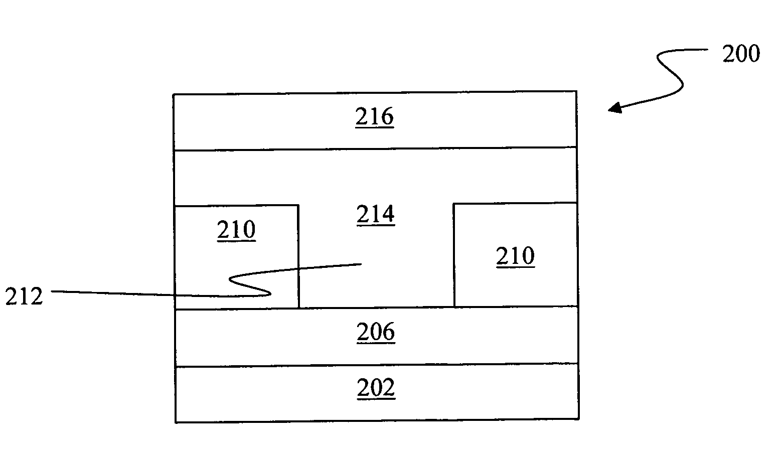
One of the significant practical challenges faced by programmable resistance memory and switching devices is a desire to reduce the contact area of the active material with one or more electrodes that contact the active material.
Lithography is commonly used to define small-scale features of semiconductor and other active material devices and often sets a limit on the goal of device miniaturization.
As the feature size of devices is minimized, however, processing of the devices becomes more difficult.
Small scale features become more difficult to define as the lithographic limit of resolution is reached and features that are defined become more difficult to process.
As the dimension or length scale of an opening decreases, it becomes increasingly difficult to satisfactorily fill the opening with another material.
Techniques such as physical vapor deposition (PVD) or sputtering fail to provide dense or complete filling of openings when the dimensions of the opening are reduced below a critical size.
Instead of providing a dense, uniform filling, these techniques increasingly incompletely fill openings as the aspect ratio (ratio of feature depth to feature lateral dimension) of the opening increases.
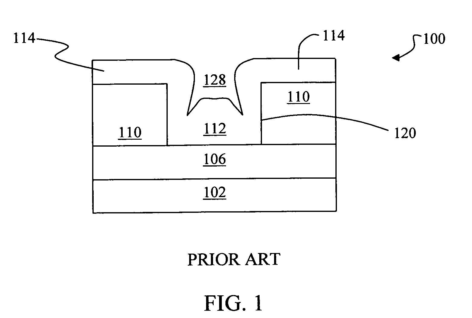
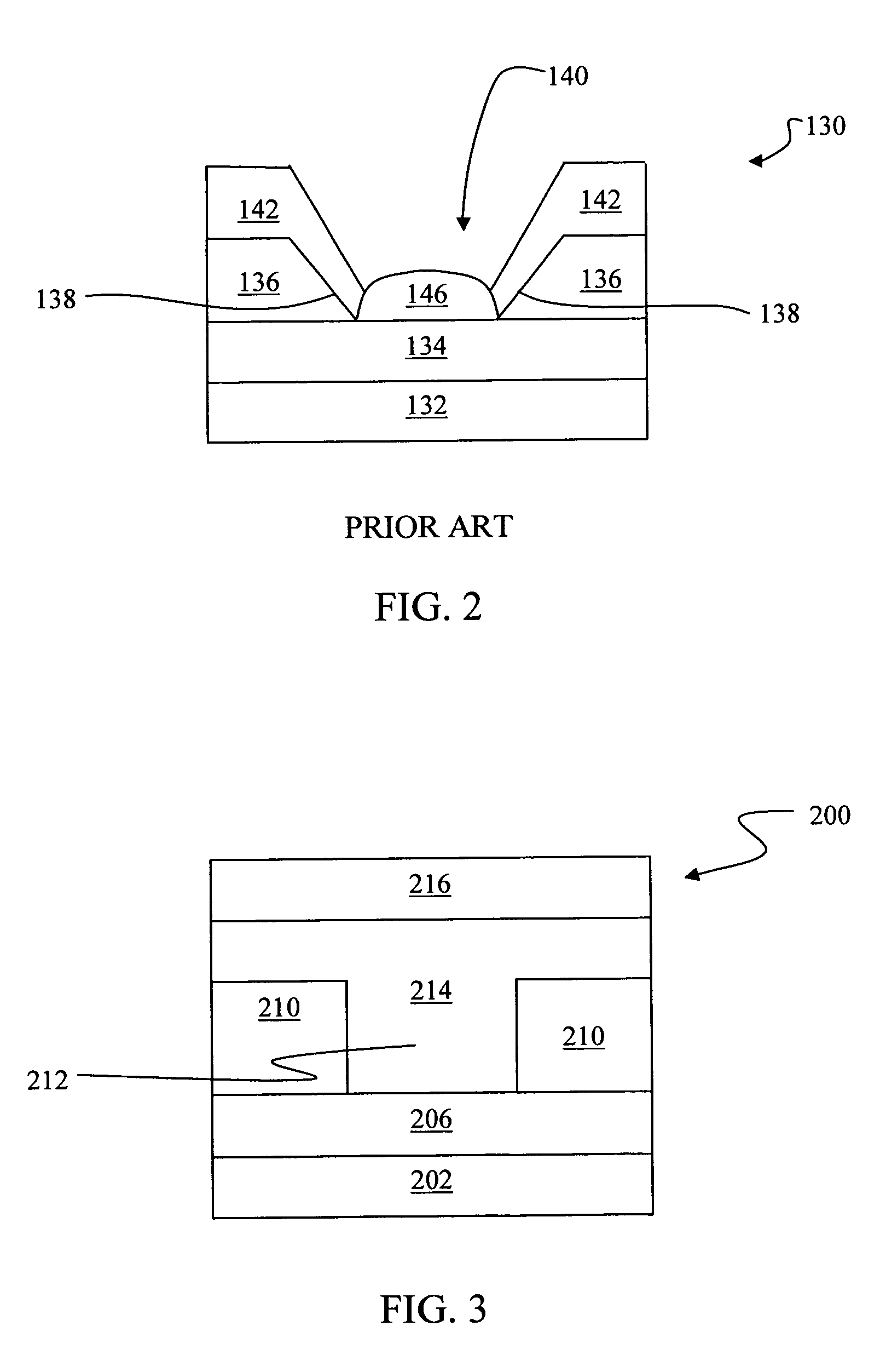
Lack of structural uniformity in the filling of openings compromises device performance due to both variations across the devices of an array and less than optimal performance from individual devices due to the defective nature of the deposited material.
Deep, narrow channels, for example, are more difficult to uniformly fill than channels that are shallow and wide.
Delivery of material, for example, to the bottom of a high aspect ratio feature becomes difficult.
Dense or complete filling of a high aspect ratio feature also becomes difficult because of the tendency for material to aggregate at or near the top of the feature during deposition.
Incomplete or non-uniform filling of the opening

Method used


Image

  • Pressure extrusion method for filling features in the fabrication of electronic devices
  • Pressure extrusion method for filling features in the fabrication of electronic devices
  • Pressure extrusion method for filling features in the fabrication of electronic devices

Examples


Example

[0040]The making and using of the presently preferred embodiments are discussed in detail below. It should be appreciated, however, that the present invention provides many applicable inventive concepts that can be embodied in a wide variety of specific contexts. The specific embodiments discussed are merely illustrative of specific ways to make and use the invention, and do not limit the scope of the invention.

[0041]Various intermediate stages of manufacturing an electronic device including a step of filling an opening within an insulating material are illustrated in FIGS. 1 through 7. The figures include stages representative of the prior art and stages in accordance with the instant invention that highlight advantages of the methods described herein. Throughout the various views and illustrative embodiments of the instant invention, like reference numbers are used to designate like elements.

[0042]The instant invention improves the uniformity, coverage, and structural characterist...


PUM


Abstract

A method of filling high aspect ratio features with active electronic or conductive materials. In one method, high pressure extrusion is used to urge the as-deposited active or conductive material into an incompletely filled opening. In another method, a rapid thermal anneal process is used to induce reflow of the as-deposited active or conductive material into an incompletely filled opening. Both methods are also effective in densifying active or conductive materials within openings by collapsing voids that arise in the as-deposited state. The instant methods provide for more uniform and consistent filling of openings and minimize the variability and impairment of electrical characteristics of active material devices. Active materials include phase-change materials, chalcogenide materials, switching materials, and programmable resistance materials.

Description

FIELD OF INVENTION[0001]This invention relates generally to the filling of openings and other features with an active material during fabrication of electronic devices. More particularly, this invention relates to the uniform filling of openings and other features with programmable resistance or electronic switching materials. Most particularly, this invention relates to the uniform and complete filling of openings and features with phase change, chalcogenide, or switching materials via extrusion induced by high gas pressure.BACKGROUND OF THE INVENTION[0002]Programmable resistance materials and fast switching materials are two classes of promising active materials for next-generation electronic storage, computing and signal transfer devices. A programmable resistance material possesses two or more states that differ in electrical resistance. The material can be programmed back and forth between the states by providing energy to the material to induce an internal transformation of th...

Claims


Application Information

Patent Timeline
IPC IPC(8): B05D5/00
CPCH01L45/06H01L45/1233H01L45/1683H01L45/1625H01L45/144H10N70/231H10N70/026H10N70/8828H10N70/826H10N70/066
Inventor LOWREY, TYLER
Owner OVONYX
Why Eureka
Try Eureka