Power semiconductor device

a technology of semiconductor devices and semiconductor components, applied in semiconductor devices, semiconductor/solid-state device details, electrical apparatus, etc., can solve the problems of large number of connection processes, large number of wiring components for connections, complex connection processes, etc., to improve productivity, reduce cost, and reduce size

Active Publication Date: 2010-06-03
MITSUBISHI ELECTRIC CORP
View PDF7 Cites 42 Cited by
  • Summary
  • Abstract
  • Description
  • Claims
  • Application Information

AI Technical Summary

Benefits of technology

[0009]The present invention has been made to solve the above problems. The object of the present invention is to provide a power semiconductor device, with improved productivity and reduced cost owing to the reduced size and simplified wiring thereof, which uses power semiconductor modules sealed with resin by transfer molding.

Problems solved by technology

Thus, since the connection is performed for each power semiconductor module and for each of the multiple terminals, the number of wiring components for the connections is large, and connection processes are complex and the number of connection processes is large.
This results in low productivity of the power semiconductor device, causing a high cost.
This results in having a wide space between the power semiconductor modules, causing a problem that the power semiconductor device becomes large-sized.

Method used


Image

  • Power semiconductor device
  • Power semiconductor device
  • Power semiconductor device

Examples


first embodiment

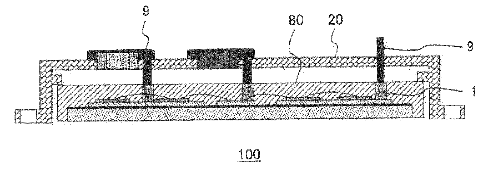
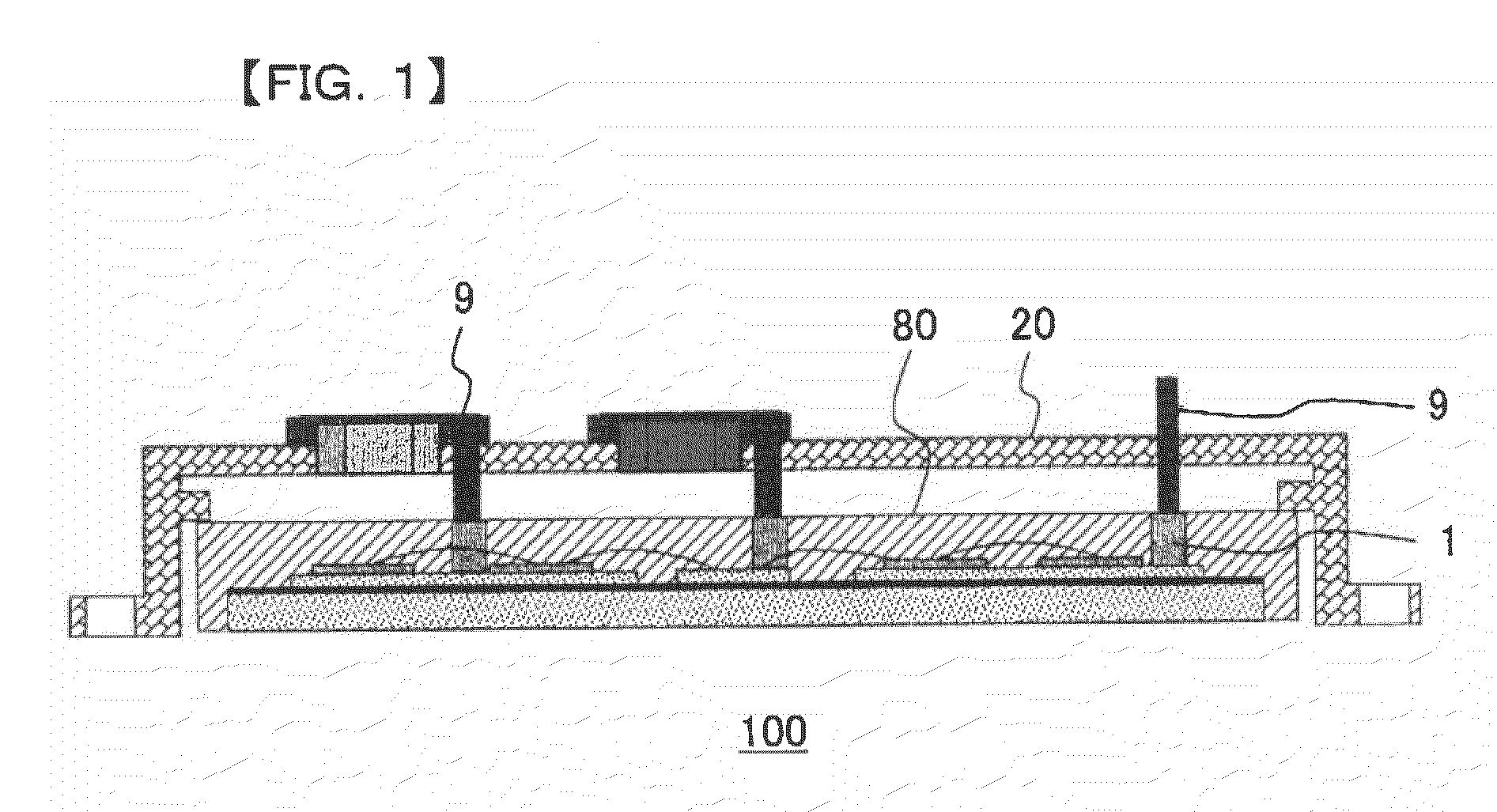
[0027]FIG. 1 is a schematic cross-sectional view showing a power semiconductor device according to the first embodiment of the present invention.

[0028]As shown in FIG. 1, in a power semiconductor device 100 of the present embodiment, a power semiconductor module 80 is set within an insert case 20. The insert case 20 is provided with external terminals 9 having portions protruding to the inside of the insert case 20. These portions are inserted and connected to cylindrical conductors 1 of the power semiconductor module 80, the cylindrical conductors 1 each having an opening at a surface of the power semiconductor module 80 (hereinafter, referred to as a top surface), the top surface facing an inner surface of the insert case 20.

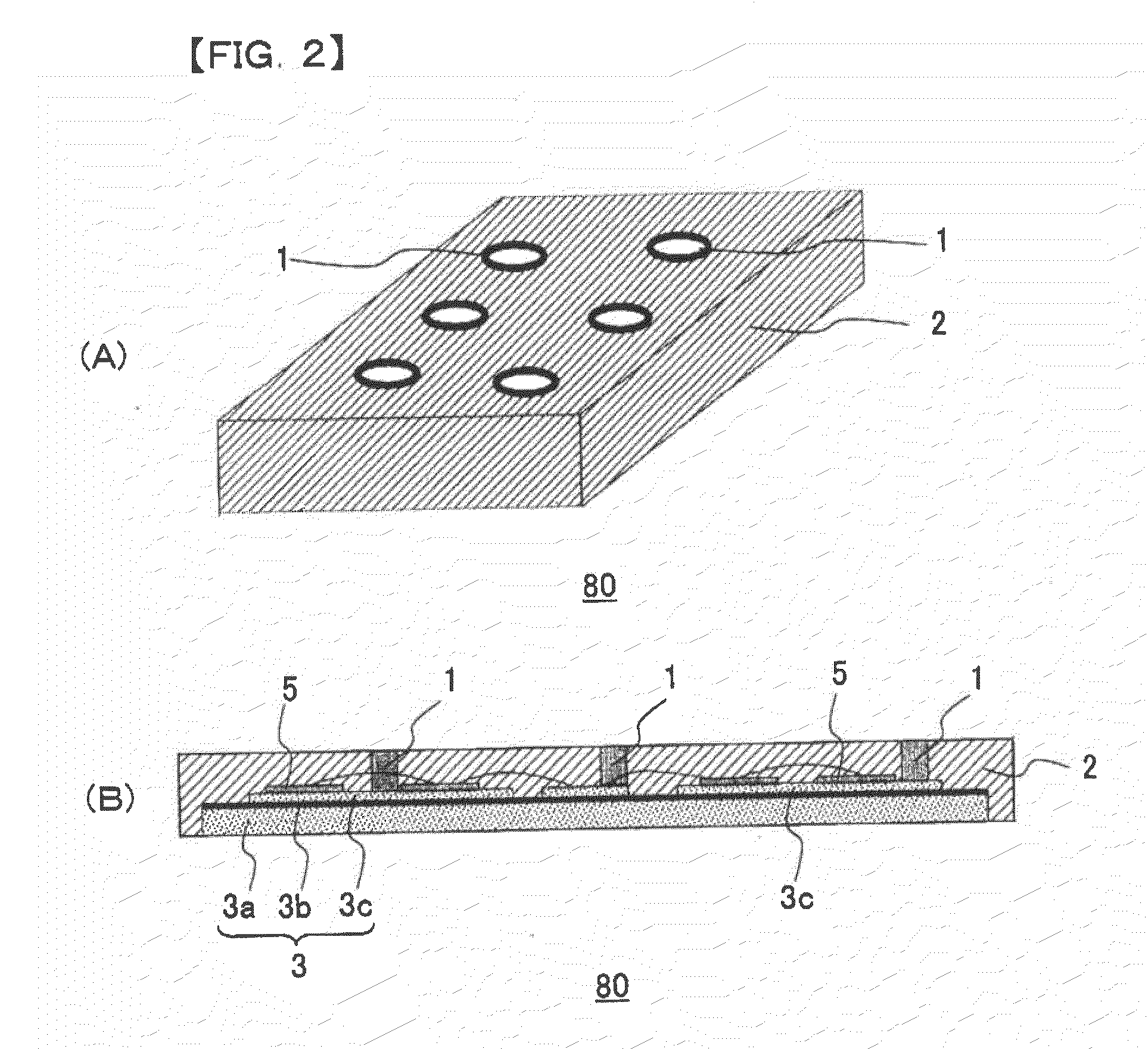
[0029]FIG. 2A is a schematic perspective view showing the power semiconductor module for use in the power semiconductor device according to the first embodiment of the present invention. FIG. 2B is a schematic cross-sectional view showing arrangement of compon...

second embodiment

[0047]FIG. 5A is a schematic perspective view showing a power semiconductor device according to the second embodiment of the present invention. FIG. 5B is a schematic perspective view showing power semiconductor modules for use in the power semiconductor device of FIG. 5A.

[0048]A power semiconductor device 200 of the present embodiment is a result of setting three power semiconductor modules 80 shown in FIG. 5B into a single insert case 30.

[0049]To be specific, although the insert case 30 used for the power semiconductor device 200 of the present embodiment is of the same type as the insert case of the first embodiment, the size of the insert case 30 allows the three power semiconductor modules 80 to be set therein at the same time. A ceiling portion 30a of the insert case 30 is provided with external terminals for the three power semiconductor modules 80. These external terminals are inserted and connected to the cylindrical conductors 1 provided in the power semiconductor modules ...

third embodiment

[0053]FIG. 6 is a schematic cross-sectional view showing an insert case used for a power semiconductor device according to the third embodiment of the present invention.

[0054]As shown in FIG. 6, the first external terminals 10 of an insert case 40 of the power semiconductor device of the present embodiment are each provided with a plurality of press fit structure portions 10b that are inner-surface-side connecting portions. The screw structure portion 10a, of each first external terminal 10, which is an outer-surface-side connecting portion, and the plurality of press fit structure portions 10b that are the inner-surface-side connecting portions, are connected by internal wiring 10c that is provided so as to be embedded in a ceiling portion 40a of the insert case 40.

[0055]Also, the second external terminal 11 is provided with a plurality of press fit structure portions 11b that are inner-surface-side connecting portions. The rod structure portion 11a that is an outer-surface-side co...


PUM


Abstract

A power semiconductor device includes a power semiconductor module having cylindrical conductors which are joined to a wiring pattern so as to be substantially perpendicular to the wiring pattern and whose openings are exposed at a surface of transfer molding resin, and an insert case having a ceiling portion and peripheral walls, the ceiling portion being provided with external terminals that are fitted into, and passed through, the ceiling portion, the external terminals having outer-surface-side connecting portions at the outer surface side of the ceiling portion and inner-surface-side connecting portions at the inner surface side of the ceiling portion. The power semiconductor module is set within the insert case such that the inner-surface-side connecting portions of the external terminals are inserted into the cylindrical conductors.

Description

BACKGROUND OF THE INVENTION[0001]1. Field of the Invention[0002]The present invention relates to a power semiconductor device in which a power semiconductor module is used, and particularly to a power semiconductor device, with a reduced size, which is excellent in terms of productivity.[0003]2. Description of the Background Art[0004]Power semiconductor devices are required to be reduced in size and operate with a large current. One of the methods for realizing such large-current operation is to wire power semiconductor modules of the same capacity in parallel to each other, thereby realizing large-current operation.[0005]In an existing method for reducing the size of a power semiconductor device, a power semiconductor module sealed with transfer molding resin is used. Among such power semiconductor modules sealed with transfer molding resin, a power semiconductor module that particularly realizes the size reduction is the one in which: power semiconductor elements are mounted on a ...

Claims


Application Information

Patent Timeline
Patent Type & Authority Applications(United States)
IPC IPC(8): H01L23/538
CPCH01L23/041H01L23/3121H01L23/3735H01L23/49811H01L24/48H01L25/072H01L2924/30105H01L25/162H01L2224/48091H01L2224/48137H01L2924/00014H01L2924/181H01L2924/00012H01L2224/45099H01L2224/45015H01L2924/207
Inventor OKA, SEIJIOBIRAKI, YOSHIKOOI, TAKESHI
Owner MITSUBISHI ELECTRIC CORP
Why Eureka
Try Eureka