
Reset synchronisation

a technology of reset synchronisation and synchronisation time, applied in the field of data processing, can solve the problems of system reset reaching the processor that are beyond the control and sight of diagnostic circuitry, and achieve the effect of simple yet effective, and maintaining their independen

Active Publication Date: 2010-06-03
ARM LTD
View PDF12 Cites 10 Cited by
  • Summary
  • Abstract
  • Description
  • Claims
  • Application Information

AI Technical Summary

Benefits of technology

[0008]In some processors, two reset signals may be asserted independently of each other and yet one may be delayed by the system to account for certain system conditions while the other is not. The present invention addresses such a problem by providing reset control circuitry that is able to delay the deassertion of one reset signal in dependence upon the other reset signal. Thus, two reset signals that may be generated and routed independently of each other can in effect be synchronised with each other by the use of this circuitry. This provides a simple yet effective way of synchronising the two signals with each other while maintaining their independence.
[0009]In some circumstances the circuitry producing the two reset signals are developed independently of each other. For example, there may be a system reset and a diagnostic reset and in such a circumstance although the diagnostic circuitry can see the system reset it does not have access to its generation circuitry. In such a case, delays in the system reset reaching the processor are beyond the control and sight of the diagnostic circuitry. Thus, providing an apparatus that can control the diagnostic reset based not on the signals generating or modifying the system reset but on the reset itself are a simple yet effective way to address this issue.
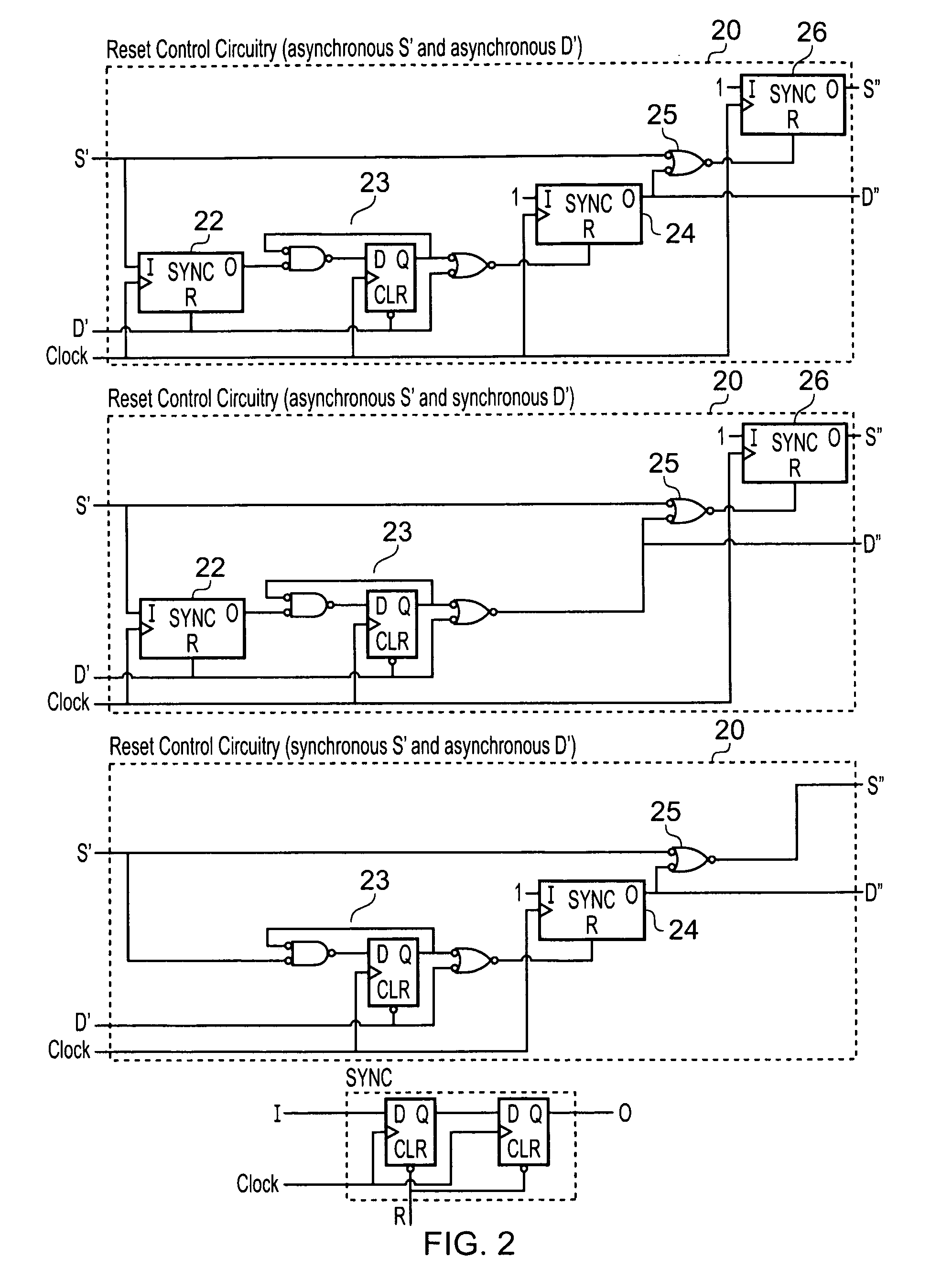
[0013]Embodiments of the present invention can also act to delay the further reset signal so that this is deasserted at a same time or later than the first reset signal that is output. The deassertion of the output first reset signal will have been delayed if the input further reset signal was asserted when it was deasserted, and it may be advantageous for the further reset signal to be asserted after or at least at the same time as the output first reset signal. Thus, where the output of the first reset signal is delayed it may also be advantageous to delay the output of the further reset signal. This could be used for example to ensure synchronisation with the circuits where the reset signals are asynchronous, or it may be used to ensure that the relative timing of the two signals is maintained.
[0031]The reset control circuitry may also be responsive to assertion of a first reset signal to automatically assert the further reset signal if it is not already asserted. This can be used to ensure certain behaviour of a circuit. For example, if the first reset signal is for a diagnostic circuit then when this is reset it may wish to diagnose the processor both during a and following on from reset and therefore, an automatic reset of the processor is generated within the reset control circuitry. As this signal is generated within the reset control circuitry, there is no asserted input further reset signal when the first reset signal is deasserted and thus, there is no delay of the first reset signal. This is advantageous as in the case of for example, a diagnostic reset it is important that it can be deasserted before the processor reset so that diagnosis through a reset can be performed.
[0033]The need to delay the first reset signal may only occur in response to the first further reset signal after power up, as it is in such a situation that issues with the further reset signal being delayed due to portions of the circuit needing to stabilise correctly occurs. Thus, it may be advantageous to provide a storage element such that the circuit can determine whether or not it is the first assertion of the further reset signal after power up and when it is not, not to delay the first reset signal.

Problems solved by technology

In such a case, delays in the system reset reaching the processor are beyond the control and sight of the diagnostic circuitry.

Method used


Image

  • Reset synchronisation
  • Reset synchronisation
  • Reset synchronisation

Examples


Embodiment Construction

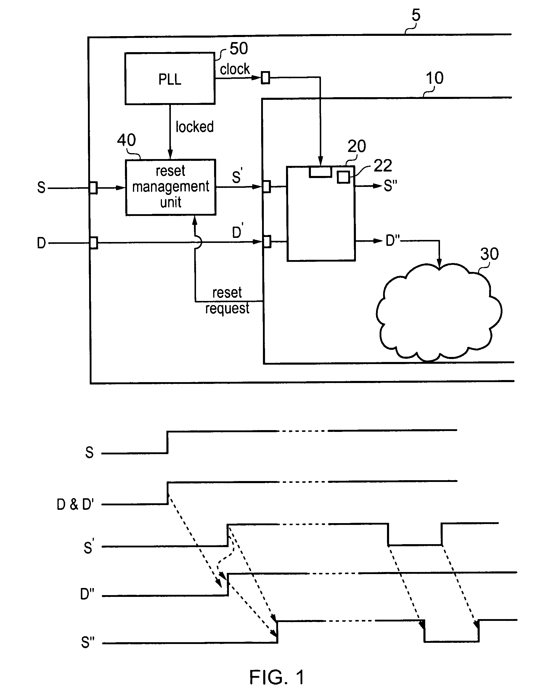
[0052]FIG. 1 shows a data processing apparatus 5 having a processor 10, reset control circuitry 20, diagnostic circuitry 30, a reset control management unit 40 and a phase locked loop 50. Data processing apparatus 5 receives a system reset signal S and a diagnostic reset signal D. These are shown as being input from outside of the data processing apparatus. They may, alternatively, be internally generated, for example in response to a power on signal.

[0053]Data processing apparatus 5 comprises reset control management unit 40 which controls the resetting of the system. When reset control management unit 40 detects the deassertion of the reset signal S it does not output the deasserted signal to processor 10 until is detects that the phase locked loop 50 which clocks processor 10 and also reset control circuitry 20 has locked. When it detects this it knows that it is safe for the processor to start operating and thus, it transmits the delayed system reset signal S′ to processor 10. T...


PUM


Abstract

Reset control circuitry is disclosed, for controlling a first reset signal for resetting at least a first portion of a circuit and a further reset signal for resetting at least a second portion of said circuit, said reset control circuitry comprising: an input for receiving an input first reset signal; an input for receiving an input further reset signal; an output for outputting an output first reset signal; and an output for outputting an output further reset signal; said reset control circuitry being responsive to detecting deassertion of said input first reset signal when said input further reset signal is asserted to delay deassertion of said output first reset signal so that said output first reset signal is deasserted at a same time or later than said input further reset signal.

Description

BACKGROUND OF THE INVENTION[0001]1. Field of the Invention[0002]The field of the invention relates to data processing and in particular to applying resets to a data processing apparatus.[0003]2. Description of the Prior Art[0004]The application of a reset to a data processing apparatus is known. This reset signal may be an asynchronous signal and therefore it may need to be synchronised to the processor's clock domain. Conventional reset synchroniser circuits are known in microprocessor designs that have a single reset input. It is also known for processors that have multiple reset inputs for these inputs to be synchronised with respect to the device they are resetting. However, there is generally no interconnection between such multiple reset inputs or their synchronisation.[0005]The application of two independent resets to a data processing apparatus is used, for example, in a processor that has some diagnostic function such as debug circuitry. Such a processor typically requires ...

Claims


Application Information

Patent Timeline
Patent Type & Authority Applications(United States)
IPC IPC(8): G06F15/177
CPCG06F1/24
Inventor GILDAY, DAVID MICHAELHARROD, PETER LOGAN
Owner ARM LTD
Learn More