Printed circuit board analyzing system, printed circuit board designing assisting system, their methods, and program

a printed circuit board and analysis system technology, applied in the direction of cross-talk/noise/interference reduction, cad circuit design, instruments, etc., can solve the problems of electromagnetic noise propagation within the printed circuit board, noise propagation throughout the printed circuit board, noise entering the input/output terminal in the lsi's to deteriorate their characteristics, etc., to achieve fast and reliable noise analysis

Inactive Publication Date: 2010-06-03
NEC CORP
View PDF9 Cites 16 Cited by
  • Summary
  • Abstract
  • Description
  • Claims
  • Application Information

AI Technical Summary

Benefits of technology

[0090]According to the present invention, an equivalent circuit model of a printed circuit board having a plurality of plane pairs and an adjacent interference part can be instantly created and a voltage value at a specified observation point can be calculated. This is very important in circuit design applications or EMC applications in which quick and highly reliable noise analysis is required.
[0091]Moreover, recommended via positioning can be calculated for suppressing interference in a printed circuit board having a plurality of plane pairs and an adjacent interference part. This is very important in circuit design applications or EMC applications in which noise suppression is desired.

Problems solved by technology

As electronic devices achieve a higher processing speed, a problem of electromagnetic noise propagation within a printed circuit board becomes conspicuous.
The noise propagates throughout the printed circuit board.
As a result, the noise enters input / output terminals in LSI's to deteriorate their characteristics.
Moreover, it is a main factor of a problem of EMI (leaked electromagnetic waves).
However, no reliable model has been proposed for a structure having stacked conductive planes of different shapes or having a plurality of conductive planes in the same layer.

Method used


Image

  • Printed circuit board analyzing system, printed circuit board designing assisting system, their methods, and program
  • Printed circuit board analyzing system, printed circuit board designing assisting system, their methods, and program
  • Printed circuit board analyzing system, printed circuit board designing assisting system, their methods, and program

Examples


first embodiment

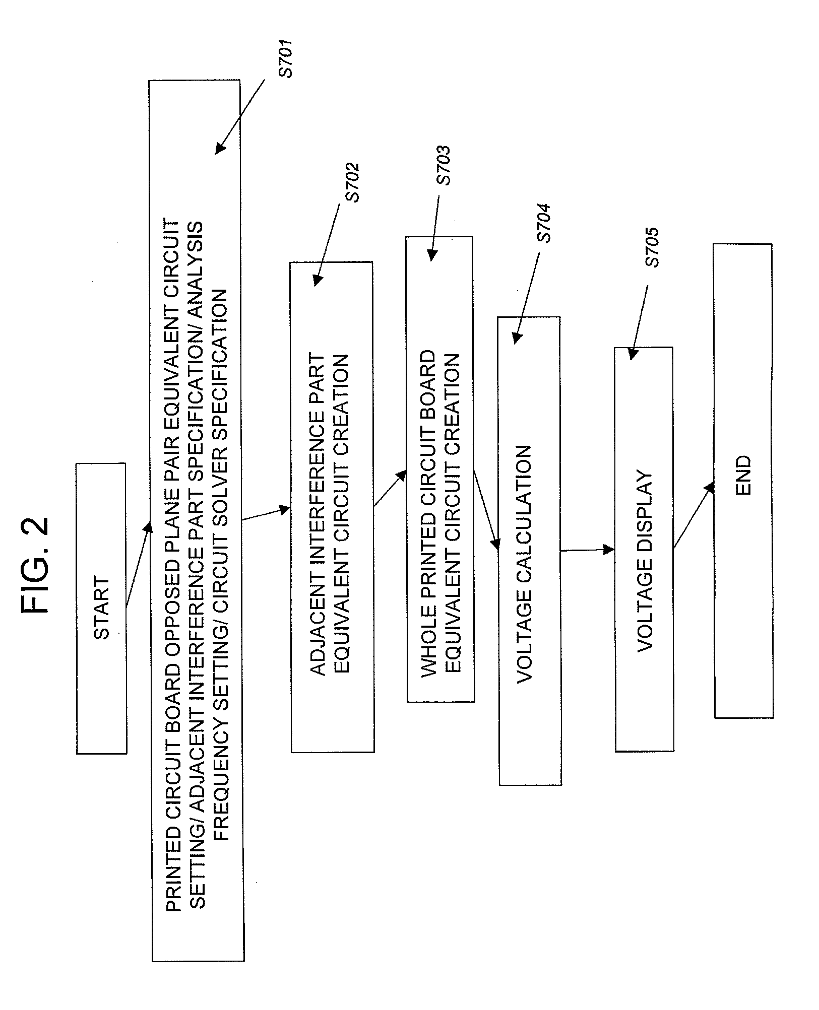
[0264]First, a printed circuit board analyzing system, a printed circuit board analyzing method and a printed circuit board analyzing program of a first embodiment in accordance with the present invention will be described.

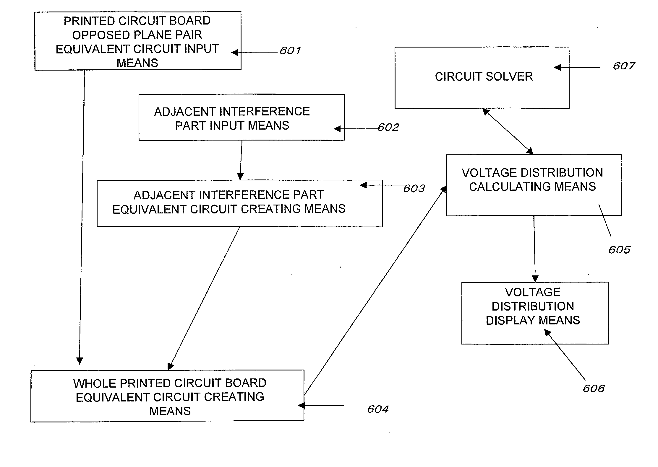
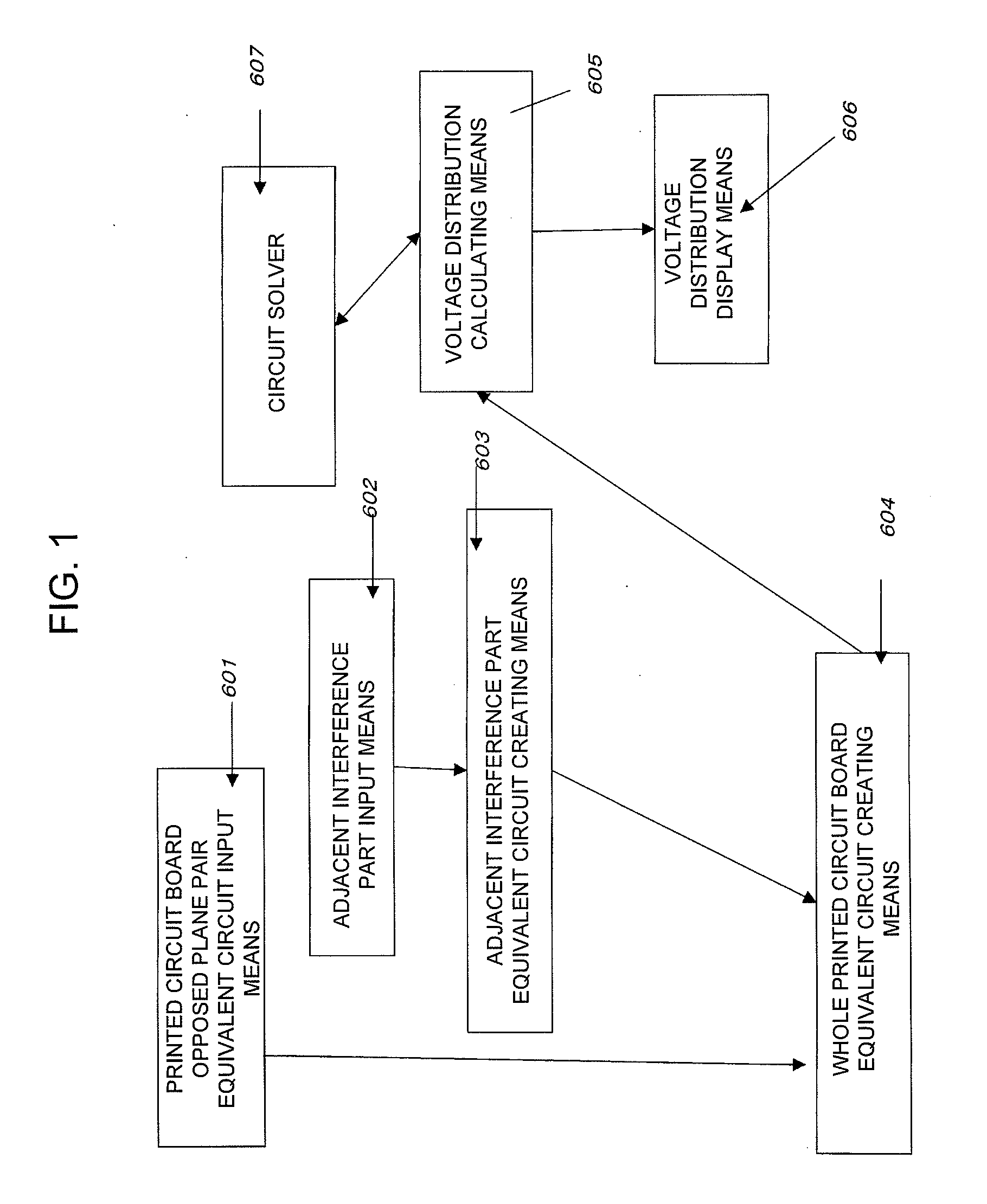
[0265]FIG. 1 is a block diagram showing a functional configuration of a printed circuit board analyzing system in accordance with the first embodiment of the present invention.

[0266]The printed circuit board analyzing system in accordance with the present invention includes printed circuit board opposed plane pair two-dimensional equivalent circuit input means 601, adjacent interference part input means 602, adjacent interference part circuit-model creating means 603, whole printed circuit board equivalent circuit creating means 604, voltage distribution calculating means 605, voltage distribution display means 606, and a circuit solver 607.

[0267]The printed circuit board opposed plane pair two-dimensional equivalent circuit input means 601 is means for inputting ...

second embodiment

[0282]Next, a printed circuit board design supporting system, a printed circuit board design supporting method and a printed circuit board design supporting program in accordance with the present invention will be described.

[0283]FIG. 9 is a block diagram showing a functional configuration of a printed circuit board design supporting system in the second embodiment of the present invention.

[0284]The printed circuit board design supporting system in the second embodiment of the present invention includes printed circuit board structure information input means 1401, mesh defining means 1402, adjacent interference via interval input means 1403, printed circuit board power-supply-plane / ground-plane extracting means 1404, adjacent interference part extracting means 1405, and adjacent interference suppressing via positioning display means 1406.

[0285]The printed circuit board structure information input means 1401 is means for inputting information about a structure of a printed circuit bo...

third embodiment

[0321]Next, a printed circuit board design supporting system, a printed circuit board design supporting method and a printed circuit board design supporting program in the present invention will be described.

[0322]FIG. 14 is a block diagram showing a functional configuration of a printed circuit board design supporting system in the third embodiment of the present invention.

[0323]The printed circuit board design supporting system in the embodiment of the present invention includes analysis evaluative printed circuit board opposed plane pair two-dimensional equivalent circuit input means 1901, analysis evaluative adjacent interference part input means 1902, analysis evaluative adjacent interference part via positioning specifying means 1903, analysis evaluative printed circuit board adjacent interference part circuit-model creating means 1904, analysis evaluative whole printed circuit board equivalent circuit creating means 1905, interference calculating means 1907, a circuit solver ...


PUM


Abstract

A printed circuit board analyzing system for analyzing the whole circuit of a multilayer printed circuit board to perform circuit analysis of noise propagation in the printed circuit board having structure in which the shapes of stacked conductor planes are different or planes are provided side by side in the same layer by quickly providing an adjacent interference part equivalent circuit model representing noise interference parts causing interference between adjacent opposed planes and by coupling the plane pairs to the adjacent interference part equivalent circuit.

Description

TECHNICAL FIELD[0001]The present invention relates to printed circuit board structures. For example, it relates to a printed circuit board analyzing system, a printed circuit board analyzing method and a printed circuit board analyzing program for efficiently handling noise propagation in a configuration constructed from a plurality of solid planes including different shapes; a printed circuit board design supporting system, a printed circuit board design supporting method and a printed circuit board design supporting program for suppressing electromagnetic interference in a printed circuit board structure constructed from a plurality of solid planes including different shapes; and printed circuit board structures.BACKGROUND ART[0002]As electronic devices achieve a higher processing speed, a problem of electromagnetic noise propagation within a printed circuit board becomes conspicuous. Electromagnetic noise (which will be referred to simply as noise hereinbelow) is caused by switch...

Claims


Application Information

Patent Timeline
Patent Type & Authority Applications(United States)
IPC IPC(8): G06F17/50
CPCG06F17/5068H05K1/0216H05K2201/09618H05K3/0005H05K2201/09309H05K1/0298G06F30/39
Inventor KOBAYASHI, NAOKI
Owner NEC CORP
Why Eureka
Try Eureka