Organic el display device and manufacturing method thereof

a display device and organic el technology, applied in the direction of organic semiconductor devices, semiconductor devices, electrical apparatus, etc., can solve the problems of cathode electrode cd being broken, defect may be produced again in some cases, and the proportion around the burr may be destroyed, so as to improve the reliability of the organic el display device having undergone a defect repair process

Active Publication Date: 2010-06-10
SAMSUNG DISPLAY CO LTD +1
View PDF1 Cites 22 Cited by
  • Summary
  • Abstract
  • Description
  • Claims
  • Application Information

AI Technical Summary

Benefits of technology

[0029]According to the method for manufacturing an organic EL display device described in (1), th...

Problems solved by technology

When electric field concentration occurs at the burr of the cathode electrode CD, the portion around the burr may be destroyed and a defect is produced again in some cases.
Further, when the repaired portion is, for exa...

Method used


Image

  • Organic el display device and manufacturing method thereof
  • Organic el display device and manufacturing method thereof
  • Organic el display device and manufacturing method thereof

Examples


Embodiment Construction

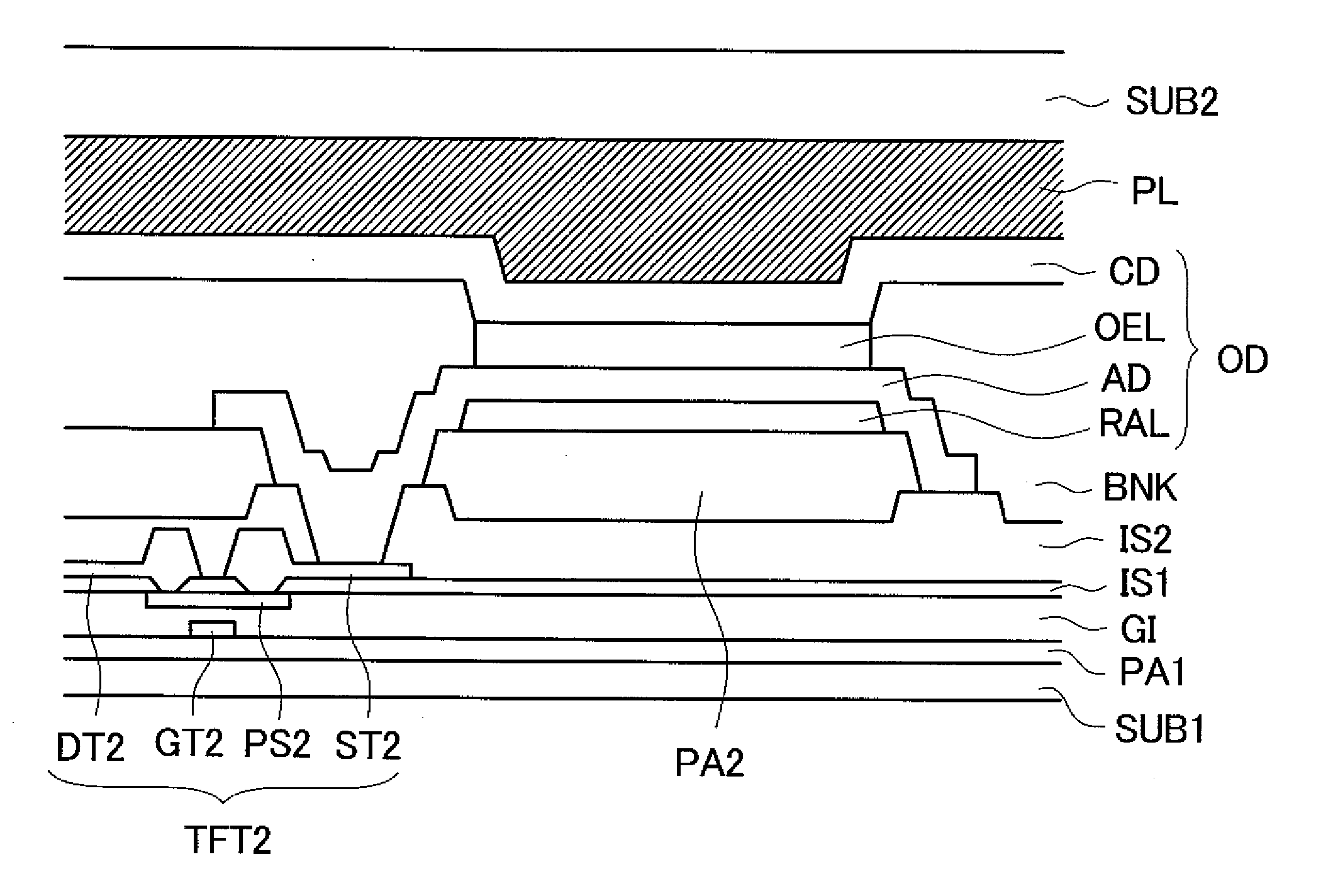
[0040]A method for manufacturing an organic EL display device according to an embodiment of the invention will be described below with reference to the drawings.

[0041]The organic EL display device in the present embodiment includes a glass substrate on which organic EL elements are formed in a matrix in correspondence with pixels and a sealing substrate to be bonded to the organic EL element substrate to seal the organic EL elements. The organic EL display device is thus formed as a top-emission device in which an image display area is formed on the side where the sealing substrate is present.

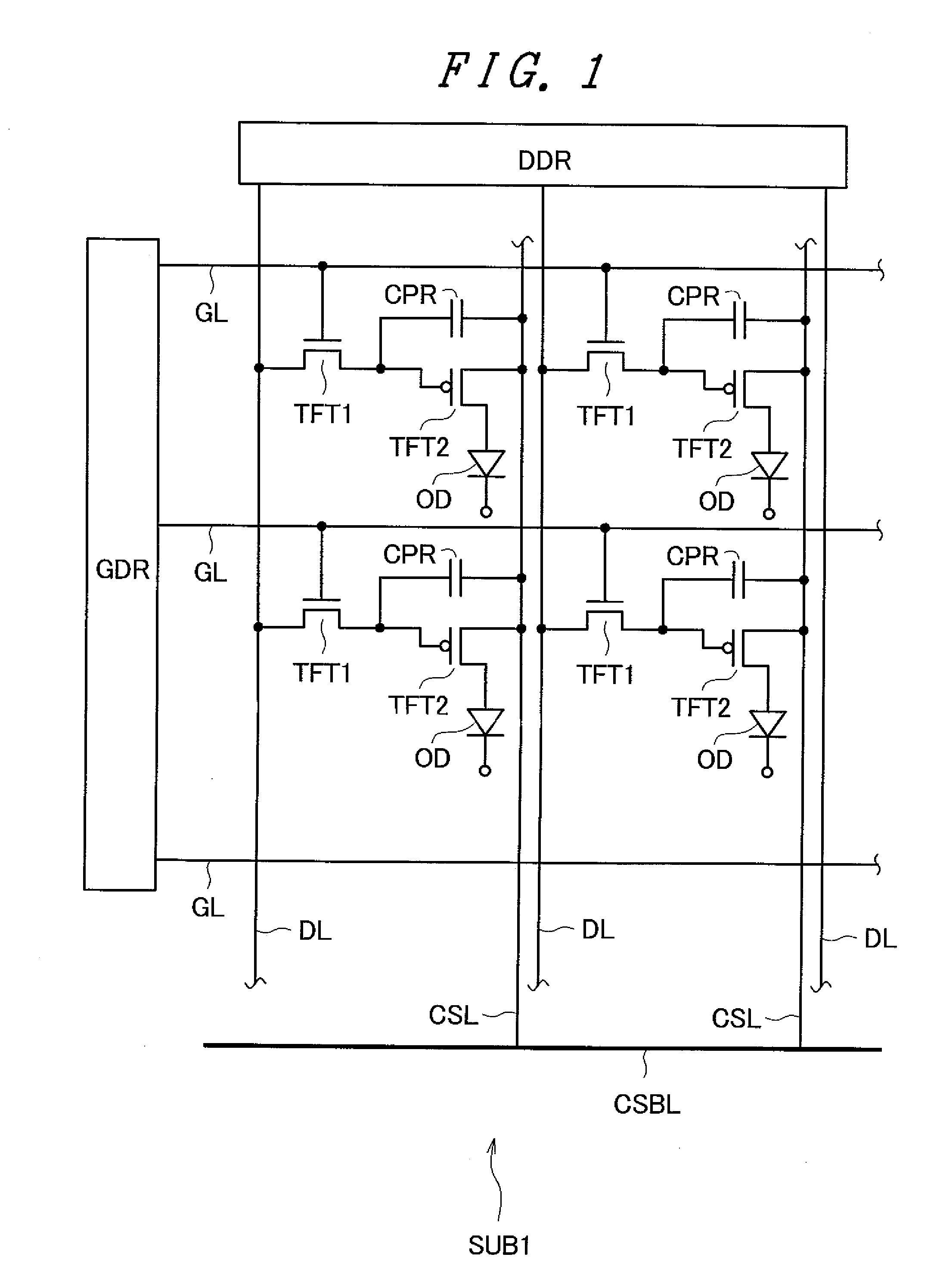
[0042]FIG. 1 is a circuit diagram showing an exemplary circuit provided on a glass substrate SUB1 in the organic EL display device described above. On the glass substrate SUB1 shown in FIG. 1, a large number of scan signal lines GL equally spaced apart from each other extend in the horizontal direction, and a large number of image signal lines DL equally spaced apart from each other extend in t...


PUM


Abstract

An object of the invention is to provide an organic EL display device manufacturing method that allows the reliability of the organic EL display device having undergone a defect repair process to be improved. A method for manufacturing an organic EL display device, the method including an organic EL element substrate formation step of forming at least one organic EL element on an organic EL element substrate, the organic EL element including an organic EL film, an anode electrode and a reflection electrode that form a first conductive film provided below the organic EL film, and a cathode electrode that forms a second conductive film provided above the organic EL film, a resin sealing step of providing a thermoplastic sealing resin to cover the upper side of the organic EL element, a defect detection step of detecting a defect in the organic EL element, and a defect elimination step of eliminating the defect detected in the defect detection step by irradiating the defect with a laser beam.

Description

CROSS-REFERENCE TO RELATED APPLICATIONS[0001]The present application claims priority from Japanese Application JP 2008-310129 filed on Dec. 4, 2008, the content of which is hereby incorporated by reference into this application.BACKGROUND OF THE INVENTION[0002]1. Field of the Invention[0003]The present invention relates a method for manufacturing an organic EL display device using organic EL elements (OLED: Organic Light-Emitting Diode) for pixel display control, and particularly to correction of defects that occur in the organic EL elements.[0004]2. Description of Related Art[0005]A contaminant X present in an organic EL film in an organic EL display device using hollow sealing technique may result in a short circuit between an anode electrode AD and a cathode electrode CD that sandwich the organic EL film in some cases. A pixel where a short circuit occurs as described above emits no light because no current flows through the organic EL film, and the entire pixel becomes a black d...

Claims


Application Information

Patent Timeline
IPC IPC(8): H01L33/00H01L21/56
CPCH01L51/5237H01L2251/568H01L51/56H10K50/8426H10K71/00H10K71/861
Inventor KAI, KAZUHIKOTANAKA, MASAHIROISHII, YOSHINORI
Owner SAMSUNG DISPLAY CO LTD
Why Eureka
Try Eureka