Chip having thermal vias and spreaders of CVD diamond

a chip and diamond technology, applied in the field of integrated circuit chips, can solve the problems of increased interconnect delay and power consumption, and achieve the effect of dispersing heat and minimizing and preferably eliminating localized hot spots

Inactive Publication Date: 2010-06-10
SEAGATE TECH LLC
View PDF8 Cites 204 Cited by
  • Summary
  • Abstract
  • Description
  • Claims
  • Application Information

AI Technical Summary

Benefits of technology

[0004]The present disclosure relates to integrated circuit chips having heat conduction paths in the chip to minimize and preferably eliminate localized ho

Problems solved by technology

As technology progresses with the desire to obtain more capacity, integrated circuit (IC) chip areas and wire lengths continue to increase, which unfortunately causes suc

Method used


Image

  • Chip having thermal vias and spreaders of CVD diamond
  • Chip having thermal vias and spreaders of CVD diamond
  • Chip having thermal vias and spreaders of CVD diamond

Examples


Embodiment Construction

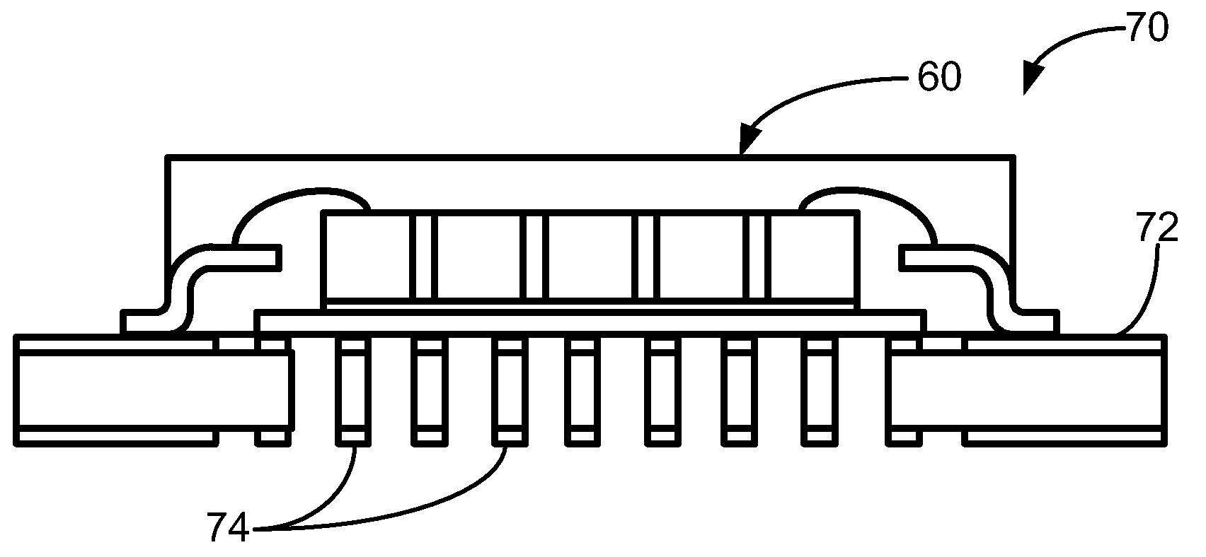
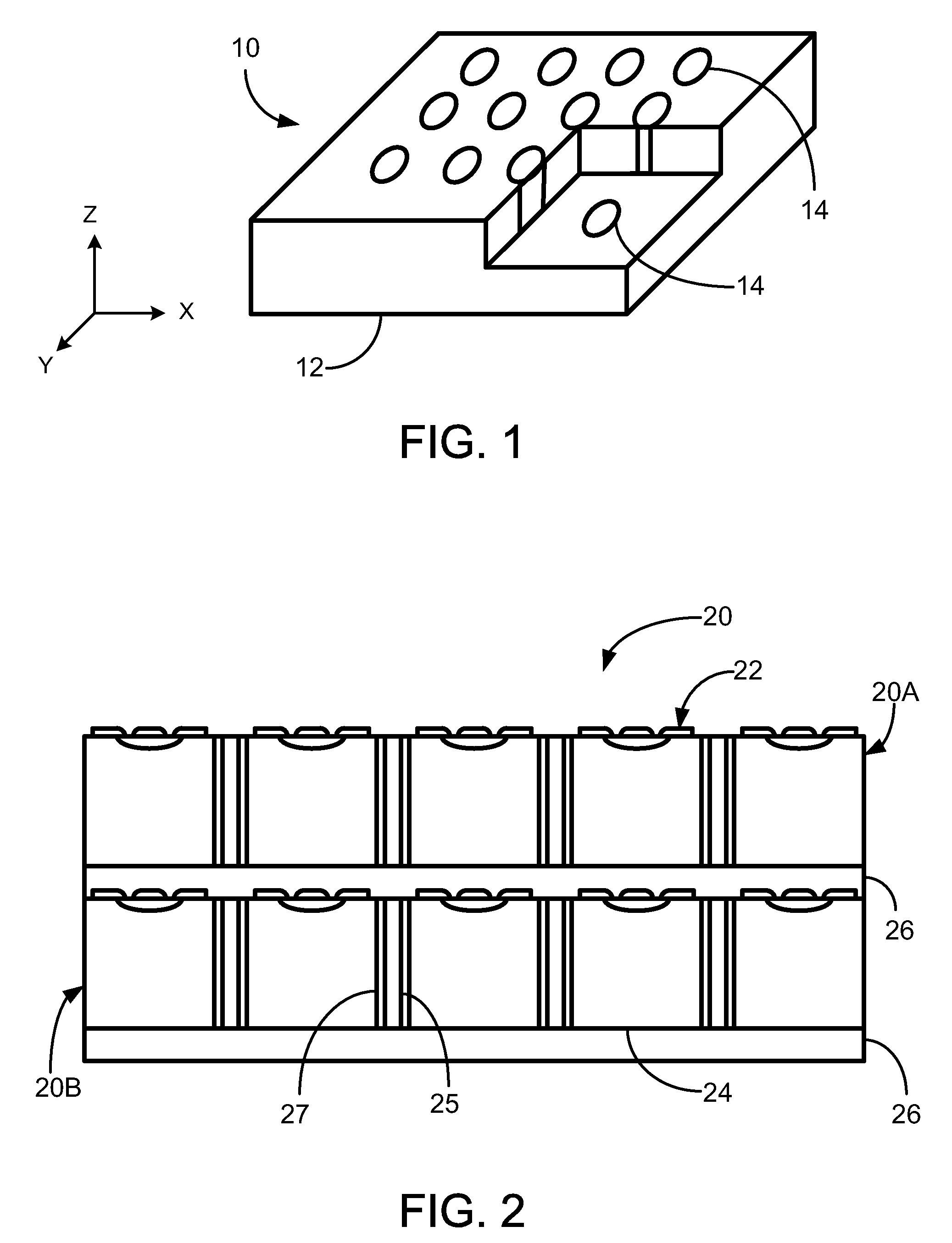
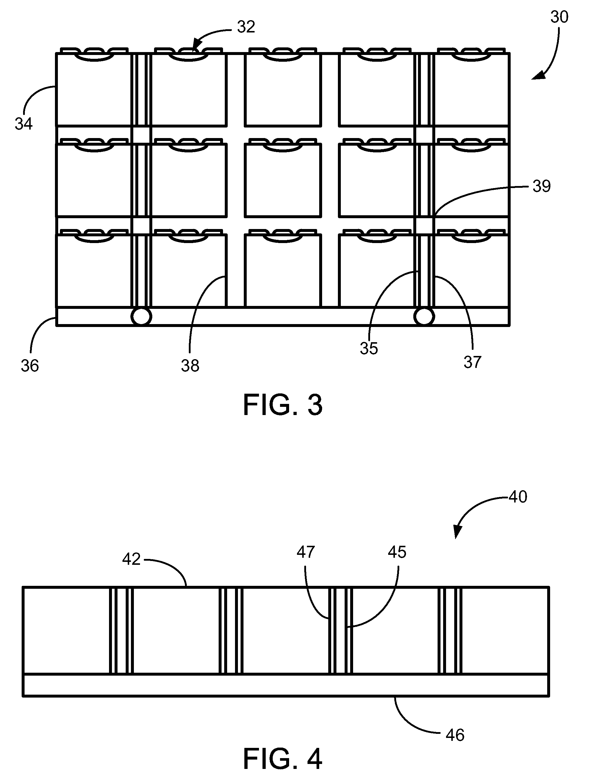
[0016]As integrated circuits (ICs) are being built vertically (i.e., three-dimensionally, 3D) to save space, thermal problems are becoming more evident and more problematic. Incorporating thermal vias into 3D integrated circuits is a manner of mitigating thermal issues by lowering the thermal resistance of the IC chip itself. By utilizing thermal vias and / or thermal spreaders, localized hot spots are inhibited and typically eliminated due to direct heat conduction paths through the thermal vias and / or spreaders. The thermal vias and spreaders are formed from chemical-vapor-deposition (CVD) diamond.

[0017]In the following description, reference is made to the accompanying set of drawings that form a part hereof and in which are shown by way of illustration several specific embodiments. It is to be understood that other embodiments are contemplated and may be made without departing from the scope or spirit of the present disclosure. The following detailed description, therefore, is not...


PUM


Abstract

An integrated circuit chip having a heat spreader comprising CVD diamond extending along the chip support body and thermal vias extending through the support body in regions free of active devices or functional elements. The thermal vias may thermally conductive and electrically conductive or may be thermally conductive and electrically resistive. The integrated circuit chips may be 3D integrated circuit chips.

Description

RELATED APPLICATION[0001]This application claims priority to U.S. provisional patent application No. 61 / 120,176, filed on Dec. 5, 2008 and titled “3D IC Thermal Via Using CVD Diamond”. The entire disclosure of application No. 61 / 120,176 is incorporated herein by reference.BACKGROUND[0002]As technology progresses with the desire to obtain more capacity, integrated circuit (IC) chip areas and wire lengths continue to increase, which unfortunately causes such problems as increased interconnect delays, power consumption, and temperature, all of which can have serious implications on reliability, performance, and design effort. Three dimensional (3D) IC technology attempts to overcome some of these limitations by stacking multiple active layers into a monolithic structure, using special processing technologies such as silicon-on-insulator (SOI) or wafer bonding. By expanding vertically rather than spreading out over a larger area, the chip space is better utilized, interconnects are decr...

Claims


Application Information

Patent Timeline
IPC IPC(8): H01L23/373H01L23/48H01L23/52
CPCH01L23/3677H01L23/3732H01L2924/1305H01L2924/01019H01L24/48H01L23/49551H01L25/0657H01L2224/48091H01L2224/48247H01L2225/06589H01L2924/01079H05K1/0206H05K3/42H05K2201/10689H01L2924/00014H01L2924/00H01L2924/14H01L2924/181H01L2224/73265H01L2924/00012H01L2224/45099H01L2224/45015H01L2924/207
Inventor SETIADI, DADILIU, HONGYUE
Owner SEAGATE TECH LLC
Why Eureka
Try Eureka