Color filter touch sensing substrate and display panel and manufacturing methods of the same

a technology of touch sensing substrate and display panel, which is applied in the manufacture of electrode systems, electric discharge tubes/lamps, instruments, etc., can solve the problems of affecting the slimness and lightness of lcd, increasing the overall thickness, and difficulty in material development, so as to reduce the touch signal and small touch sensing area

Active Publication Date: 2010-06-17
AU OPTRONICS CORP
View PDF10 Cites 153 Cited by
  • Summary
  • Abstract
  • Description
  • Claims
  • Application Information

AI Technical Summary

Benefits of technology

[0008]The present invention provides a color filter touch sensing substrate and a manufacturing method thereof The present invention can solve a problem

Problems solved by technology

Obviously, the touch sensing substrate in the plug in touch sensing panel increases an overall thickness and adversely affects the slimness and lightness of the LCD.
However, this method has a difficulty in material development as a material with high hardness and stability is required to avoid scratches and increase manufacturing efficiency.
In addition, a failure to slim a color filter glass substr

Method used


Image

  • Color filter touch sensing substrate and display panel and manufacturing methods of the same
  • Color filter touch sensing substrate and display panel and manufacturing methods of the same
  • Color filter touch sensing substrate and display panel and manufacturing methods of the same

Examples


Embodiment Construction

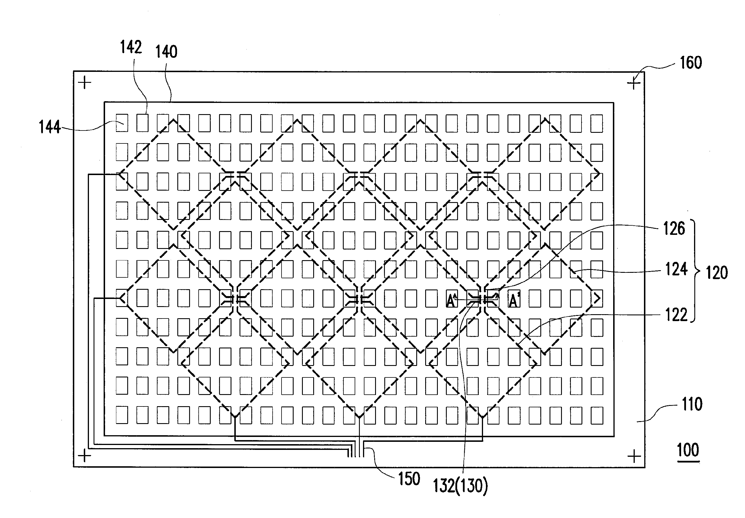
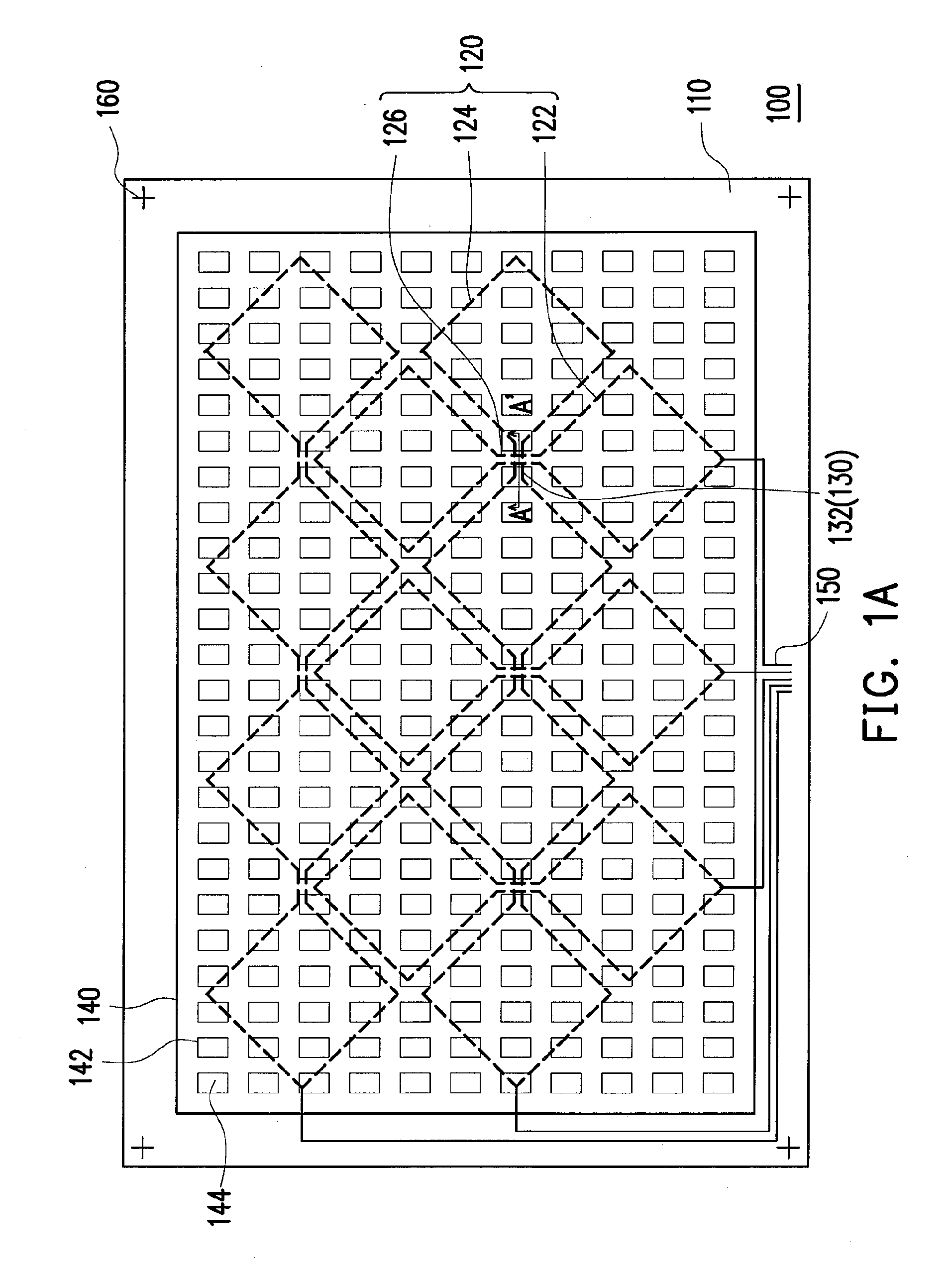
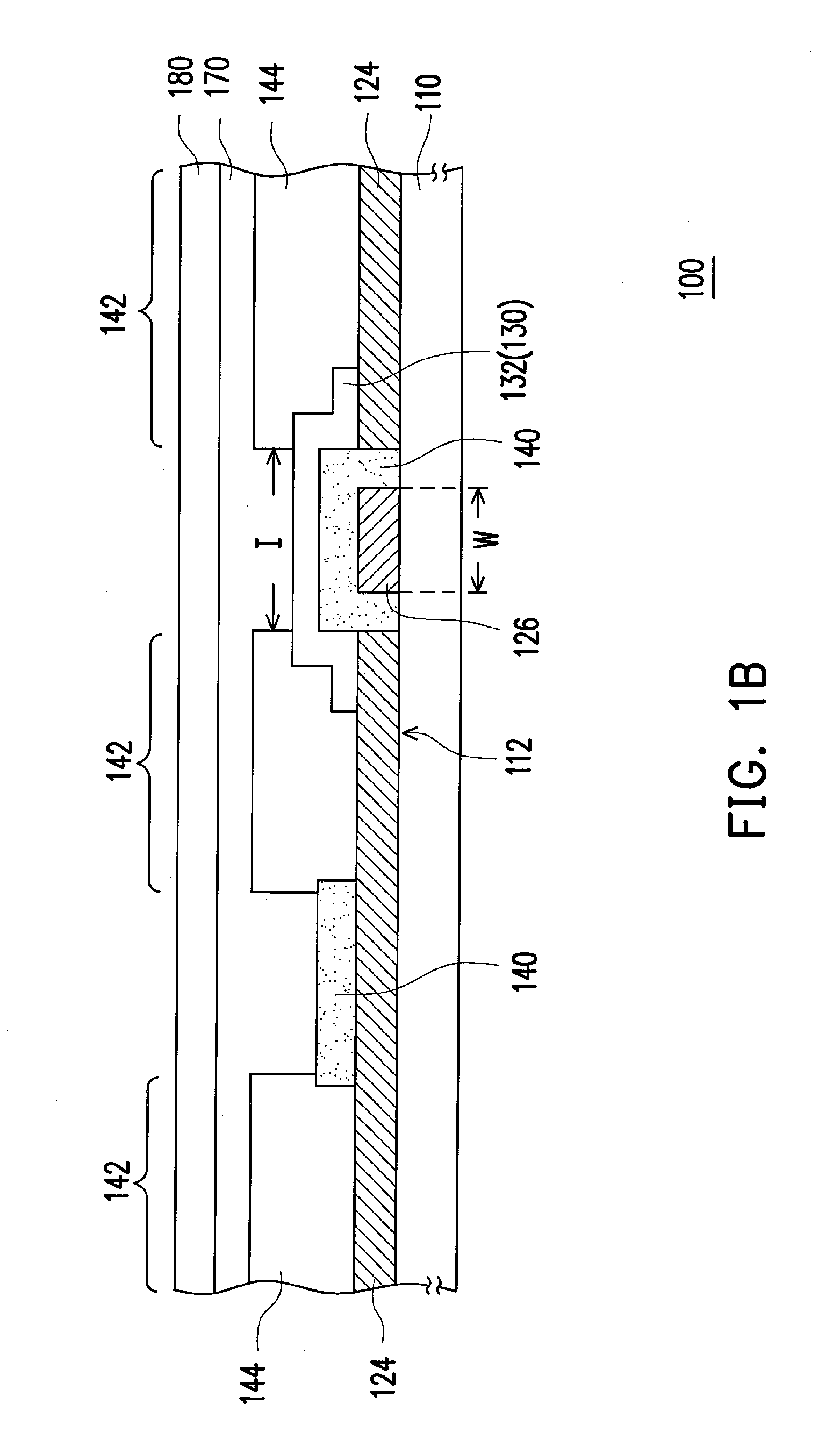
[0043]FIG. 1A is a top view of a color filter touch sensing substrate according to an embodiment of the present invention. FIG. 1B is a cross-sectional view of FIG. 1A along line A-A′. Referring to FIG. 1A and FIG. 1B simultaneously, a color array substrate 100 in the present embodiment includes a first film 120, a second film 130, a light shielding pattern layer 140, and a plurality of color filter pattern layers 144.

[0044]The first film 120 is a first conductive pattern layer which is disposed on a substrate 110. The first film 120 includes a plurality of first touch sensors 122, a plurality of second touch sensors 124, and a plurality of first bridge lines 126 used to electrically connect the first touch sensors 122 in the same column. A material of the first film 120 is a transparent conductive material, for example, indium tin oxide (ITO) or indium zinc oxide (IZO), etc.

[0045]Moreover, the second film 130 is a second conductive pattern layer which includes a plurality of second...


PUM


Abstract

A manufacturing method of a color filter touch sensing substrate is provided. Firstly, a first film is formed on a substrate. The first film includes a plurality of first and second touch sensors and a plurality of first bridge lines for electrically connecting the first touch sensors in the same column. Then, a second film is formed on the substrate. The second film includes a plurality of second bridge lines for electrically connecting the second touch sensors in the same row. Next, a light shielding pattern layer is formed between the first and the second films. The light shielding pattern layer is used to define a plurality of sub-pixel regions on the substrate. Afterward, a plurality of color filter pattern layers is formed in the sub-pixel regions. Furthermore, a color filter touch sensing substrate, a display panel and manufacturing methods thereof are also provided.

Description

CROSS-REFERENCE TO RELATED APPLICATION[0001]This application claims the priority benefit of Taiwan application serial no. 97148273, filed Dec. 11, 2008. The entirety of the above-mentioned patent application is hereby incorporated by reference herein and made a part of specification.BACKGROUND OF THE INVENTION[0002]1. Field of the Invention[0003]The present invention relates to a color filter touch sensing substrate, a display panel and manufacturing methods of the same. More particularly, the present invention relates to a color filter touch sensing substrate using a light shielding pattern layer to separate bridge lines of adjacent touch sensors, a display panel, and manufacturing methods of the same.[0004]2. Description of Related Art[0005]Touch sensing panels can be categorized into resistance touch sensing panels, capacitance touch sensing panels, optical touch sensing panels, sound wave touch sensing panels, and electromagnetic touch sensing panels, etc, based on differences i...

Claims


Application Information

Patent Timeline
IPC IPC(8): G06F3/041H01J9/00
CPCG06F3/0412G02F1/133514G06F3/045
Inventor CHIEN, YU-FENGYANG, TUN-CHUNLEE, SEOK-LYULHUANG, WEI-MING
Owner AU OPTRONICS CORP
Why Eureka
Try Eureka