Method for bonding two substrates

a technology of substrates and substrates, applied in the direction of electrical equipment, semiconductor devices, radio frequency controlled devices, etc., can solve the problems of fast and easy process, reduce and achieve fast and easy process. , the effect of reducing the number of edge voids

Inactive Publication Date: 2010-06-24
S O I TEC SILICON ON INSULATOR THECHNOLOGIES
View PDF48 Cites 22 Cited by
  • Summary
  • Abstract
  • Description
  • Claims
  • Application Information

AI Technical Summary

Benefits of technology

[0007]It is the surprising finding of this invention that it is the combination of the two steps a) and b) that leads to the desired level in the bonding energy, namely of the order of 700 to 1000 mJoule / m2 with a reduced number of edge voids compared to known bonding processes. Furthermore, by only applying a partial vacuum, which can easily be reached by using standard rough pumps only, the process is fast and easy to carry out. A high bonding quality, namely no edge voids or at least a reduced number of edge voids, can be achieved even with two substrates having thermal expansion coefficients which are so different that the standard thermal anneal methods cannot be applied.
[0008]Finally, the bonding quality observed with the inventive method is sufficient to carry out a layer transfer according to the Smart Cut™ layer transfer technology, where ions are implanted into a donor wafer to define a plane of weakness. The bonded assembly comprising the donor wafer can then be split in the absence or with a reduced number of edge defects and despite the use of relatively low temperatures.

Problems solved by technology

Furthermore, by only applying a partial vacuum, which can easily be reached by using standard rough pumps only, the process is fast and easy to carry out.

Method used


Image

  • Method for bonding two substrates
  • Method for bonding two substrates

Examples


Embodiment Construction

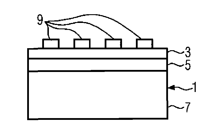
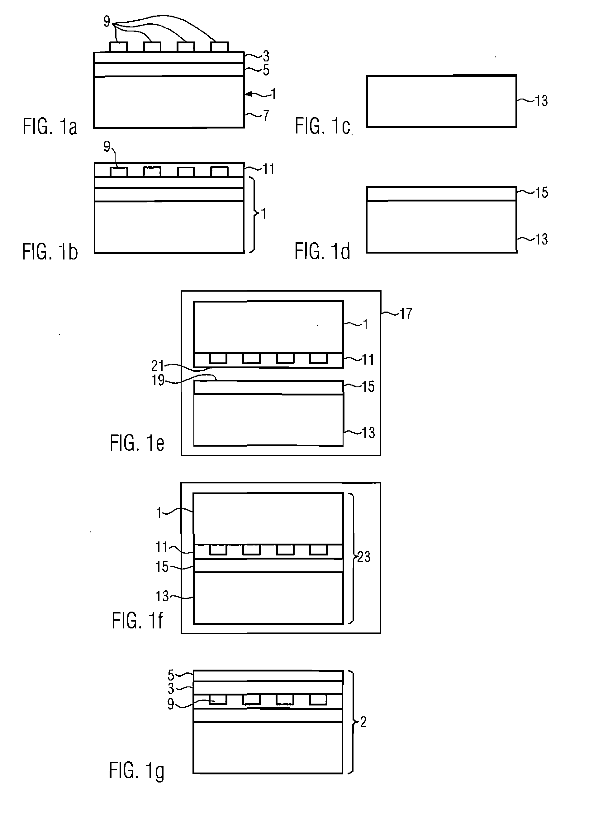
[0012]In this invention, at least one of the two substrates can comprise processed or at least partially processed devices. In this context, the term “device” relates to any structure on at least one of the substrates which at least partially belongs to the final devices such as electronic devices or opto-electronic devices comprising, amongst others, capacitor and / or transistor structures. It is the particular advantage of the invention that it can be applied to any bonded structure that requires high bonding energy but cannot be exposed to high temperature and / or that suffers from the presence of edge voids. This is the case when devices are present in or on one of the substrates.

[0013]According to an advantageous embodiment of the invention, the partial vacuum used in the contacting step can have a pressure of 1 to 50 Torr (1.33 to 66.7 mbar), preferably 1 to 20 Torr (1.33 to 26.6 mbar), preferably between 10 to 20 Torr (13.3 to 26.6 mbar). This level of vacuum can be easily and ...


PUM


Abstract

The invention relates to a method for bonding two substrates by applying an activation treatment to at least one of the substrates, and performing the contacting step of the two substrates under partial vacuum. Due to the combination of the two steps, it is possible to carry out the bonding and obtain high bonding energy with a reduced number of bonding voids. The invention is in particular applicable to a substrate of processed or at least partially processed devices.

Description

TECHNICAL FIELD[0001]The invention relates to a method for bonding two substrates, and in particular to a method wherein at least one of the two substrates may comprise processed or at least partially processed devices. This kind of bonding situation occurs, for example, in the fabrication process of backside illuminated CMOS imager structures, when a first substrate comprising the opto-electronic devices of the CMOS imager are bonded to a second substrate. After bonding, the first substrate is thinned, preferentially by grinding, so that light can enter into the device via the backside.[0002]During bonding, the adhesion between two substrates is achieved via molecular forces (Van de Waals forces). To achieve a high quality bonding and to facilitate the subsequent thinning step, it is mandatory to obtain a high bonding energy, at least in the range of 700 to 1000 mJ / m2 or even more. In the prior art, high bonding energies are obtained by heating the assembled structure, typically to...

Claims


Application Information

Patent Timeline
Patent Type & Authority Applications(United States)
IPC IPC(8): H01L27/12H01L21/762
CPCH01L21/76256H01L27/146
Inventor CASTEX, ARNAUD
Owner S O I TEC SILICON ON INSULATOR THECHNOLOGIES
Why Eureka
Try Eureka