Color electrophoretic display device and method for manufacturing the same

a display device and electrophoretic technology, applied in non-linear optics, instruments, optical elements, etc., can solve the problems of reducing image quality, damage to expensive electronic ink films, and reducing image quality, so as to achieve the effect of reducing the cost of electronic ink films and reducing the cost of ink films

a display device and electrophoretic technology, applied in non-linear optics, instruments, optical elements, etc., can solve the problems of reducing image quality, damage to expensive electronic ink films, and reducing image quality, so as to achieve the effect of reducing the cost of electronic ink films and reducing the cost of ink films

US20100157411A1Inactive Publication Date: 2010-06-24LG DISPLAY CO LTD

Image

  • Color electrophoretic display device and method for manufacturing the same
  • Color electrophoretic display device and method for manufacturing the same
  • Color electrophoretic display device and method for manufacturing the same

Examples


first embodiment

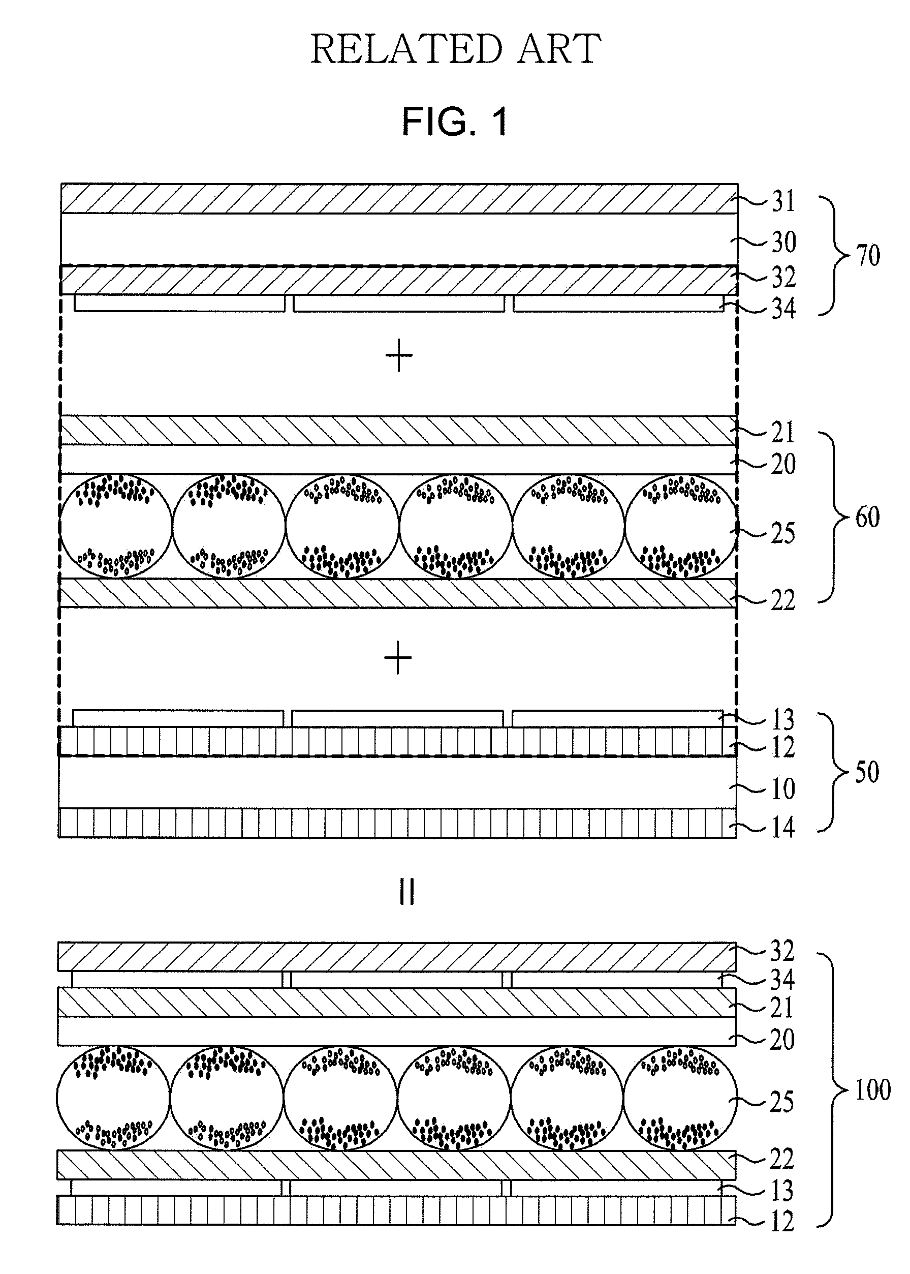
[0047]FIGS. 2A to 2C are plan views illustrating a TFT substrate, an electronic ink film, and a color filter layer during a process for manufacturing a color electrophoretic display device in accordance with the present invention, and FIGS. 3A to 3C are longitudinal-sectional views respectively corresponding to FIGS. 2A to 2C.

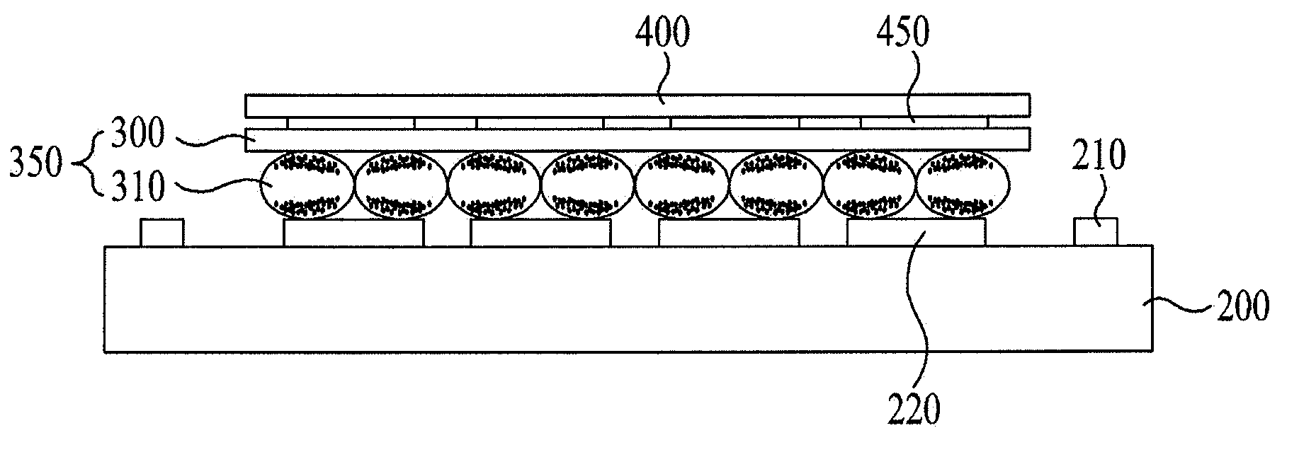
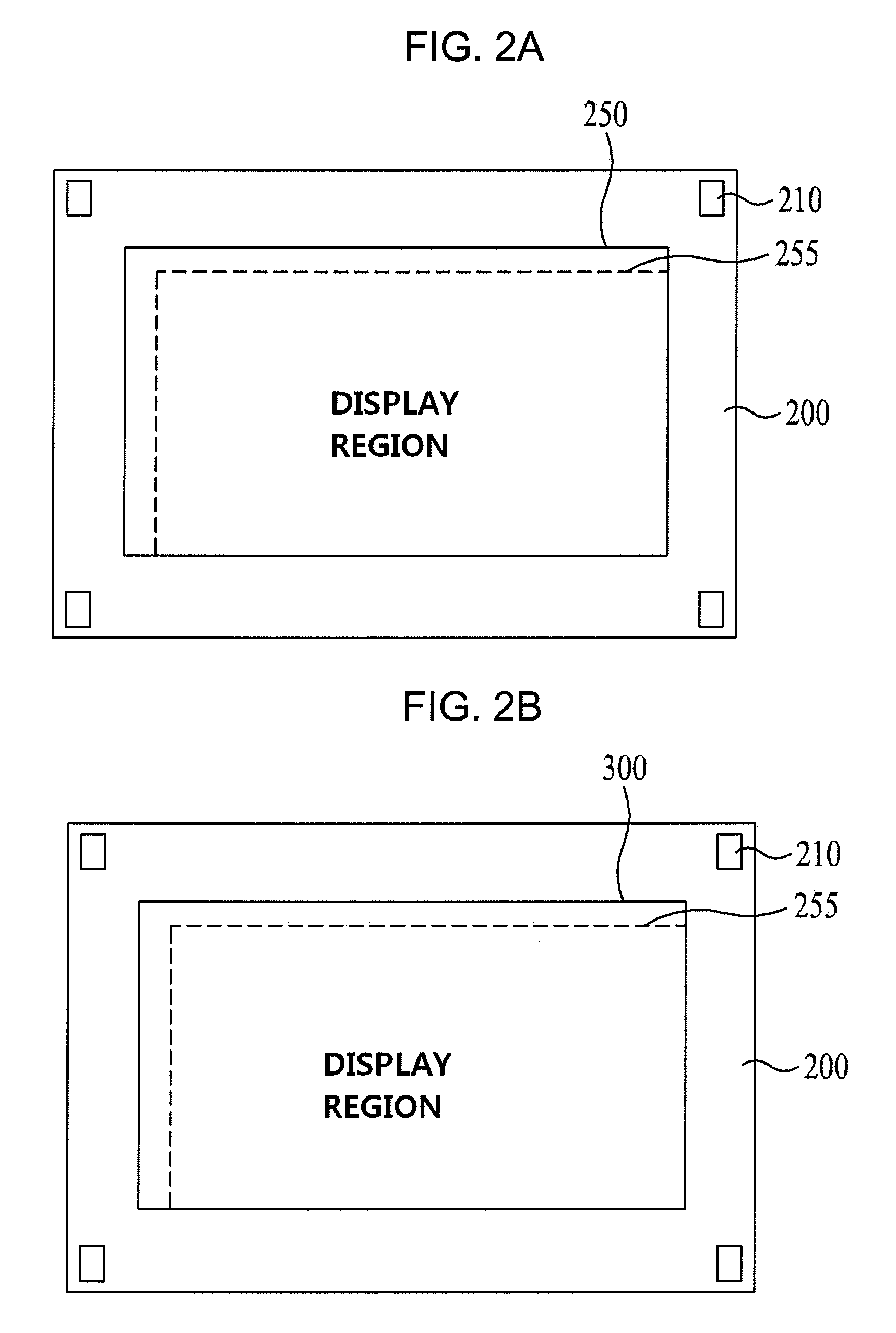
[0048]In order to manufacture the color electrophoretic display device in accordance with the first embodiment of the present invention, as shown in FIGS. 2A and 3A, a TFT array mother substrate 200 is first prepared. Here, together with TFTs 220, alignment keys 210 to sense a position of a color filter layer are formed at the edge of the TFT array mother substrate 200.

[0049]Each of the TFTs 220 includes a gate electrode 221a formed in a designated region on the TFT array mother substrate 200, a gate insulating film 227 formed over the entire surface of the substrate 220 including the gate electrode 221a, an island-type semiconductor layer 223: 223a, 223b forme...

second embodiment

[0088]FIGS. 8A to 8C are plan views illustrating a process for manufacturing a color electrophoretic display device in accordance with the present invention.

[0089]The process in accordance with the second embodiment is nearly identical with that in accordance with the first embodiment except that the color filter layer 450 in accordance with the second embodiment is formed in a quad type instead of the stripe type.

[0090]Here, reference numerals 206 and 207 in FIG. 8A represent a gate pad region and a data pad region, respectively, and from FIG. 8B, it is apparent that the substrate 300 of the electrophoretic layer 350 has an area which is slightly overlapped with the pad regions 206 and 207.

[0091]FIG. 8C shows scribing lines, along which the TFT array mother substrate 200 is cut into unit panels. Here, the alignment keys 210 may be placed in a region which is removed by the scribing process, or may remain at the outside (a part except for the display region) of the unit panel.

[0092]...


PUM


Abstract

Discussed are a color electrophoretic display device with a color filter layer, which is formed in a droplet state on a rear surface of an electronic ink film through surface treatment so as to be capable of adjusting density of droplets in pixels and achieving correct alignment, and a method for manufacturing the same. The method includes forming a thin film transistor (TFT) array substrate including a display region, in which a plurality of pixel regions are defined in a matrix, and alignment keys provided at the outside of the display region, forming an electrophoretic layer including a micro capsule layer formed so as to correspond to the display region of the TFT array substrate, and forming a color filter layer on the electrophoretic layer using the alignment keys so as to correspond to the respective pixel regions of the display region.

Description

[0001]This application claims the benefit of Korean Patent Application No. 10-2008-0132004, filed on Dec. 23, 2008, which is hereby incorporated by reference as if fully set forth herein.BACKGROUND OF THE INVENTION[0002]1. Field of the Invention[0003]The present invention relates to an electrophoretic display device, and more particularly, to a color electrophoretic display device with a color filter layer, which is formed in a droplet state on a rear surface of an electronic ink film through surface treatment so as to be capable of adjusting density of droplets in pixels and achieving correct alignment, and a method for manufacturing the same.[0004]2. Discussion of the Related Art[0005]An electrophoretic display device (EPD) is one of flat panel display device used in E-books, and includes two display panels, on which electrodes for forming an electric field are formed, and micro capsules formed between the two display panels and containing electronic ink having black and white pig...

Claims


Application Information

Patent Timeline
24 Jun 2010
Publication
US20100157411A1
IPC
G02F1/167; H01L33/00; G02F1/1677
CPC
G02F1/133514; H01L27/1214; G02F2201/52; G02F1/167; H01L27/1255; G02F1/1677
Inventors
KWON, OH-NAM; LEE, JAE-GU