Method for manufacturing transistor

a manufacturing method and transistor technology, applied in the direction of electroluminescent light sources, semiconductor/solid-state device testing/measurement, electroluminescent light sources, etc., can solve problems such as difficulty in lowering resistance, and achieve the effect of variable conductivity between the source region and the drain region

Active Publication Date: 2010-06-24
SEMICON ENERGY LAB CO LTD
View PDF99 Cites 194 Cited by
  • Summary
  • Abstract
  • Description
  • Claims
  • Application Information

AI Technical Summary

Benefits of technology

[0022]According to an embodiment of the present invention, a hydrogen barrier layer is selectively provided over an oxide semiconductor layer including hydrogen and hydrogen is selectively desorbed from a given region in the oxide semiconductor layer by conducting oxidation treatment so that regions with different conductivities are formed in the oxide semiconductor layer. With the use of the regions with different conductivities formed in the oxide semiconductor layer, a channel formation region, a source region, and a drain region can be formed. In this case, hydrogen is included in the oxide semiconductor layer in advance, so that variations in conductivity between the source region and the drain region, which are provided in the oxide semiconductor layer, can be reduced. In addition, a position where the hydrogen barrier layer is provided is controlled, so that the regions with different conductivities can be formed appropriately in the oxide semiconductor layer.

Problems solved by technology

However, it is difficult to lower resistance by diffusing hydrogen along a thickness direction of an oxide semiconductor (to a surface which is opposite to a surface in contact with a source electrode and a drain electrode of the oxide semiconductor) when hydrogen is diffused into the oxide semiconductor from the source electrode and the drain electrode.
In addition, there is a problem in that distribution of hydrogen concentration in a plane direction of an oxide semiconductor layer (a direction parallel to a substrate) depends on shapes of the source electrode and the drain electrode.

Method used


Image

  • Method for manufacturing transistor
  • Method for manufacturing transistor
  • Method for manufacturing transistor

Examples


embodiment 1

[0061]In this embodiment, an example of a method for manufacturing a transistor is described with reference to drawings.

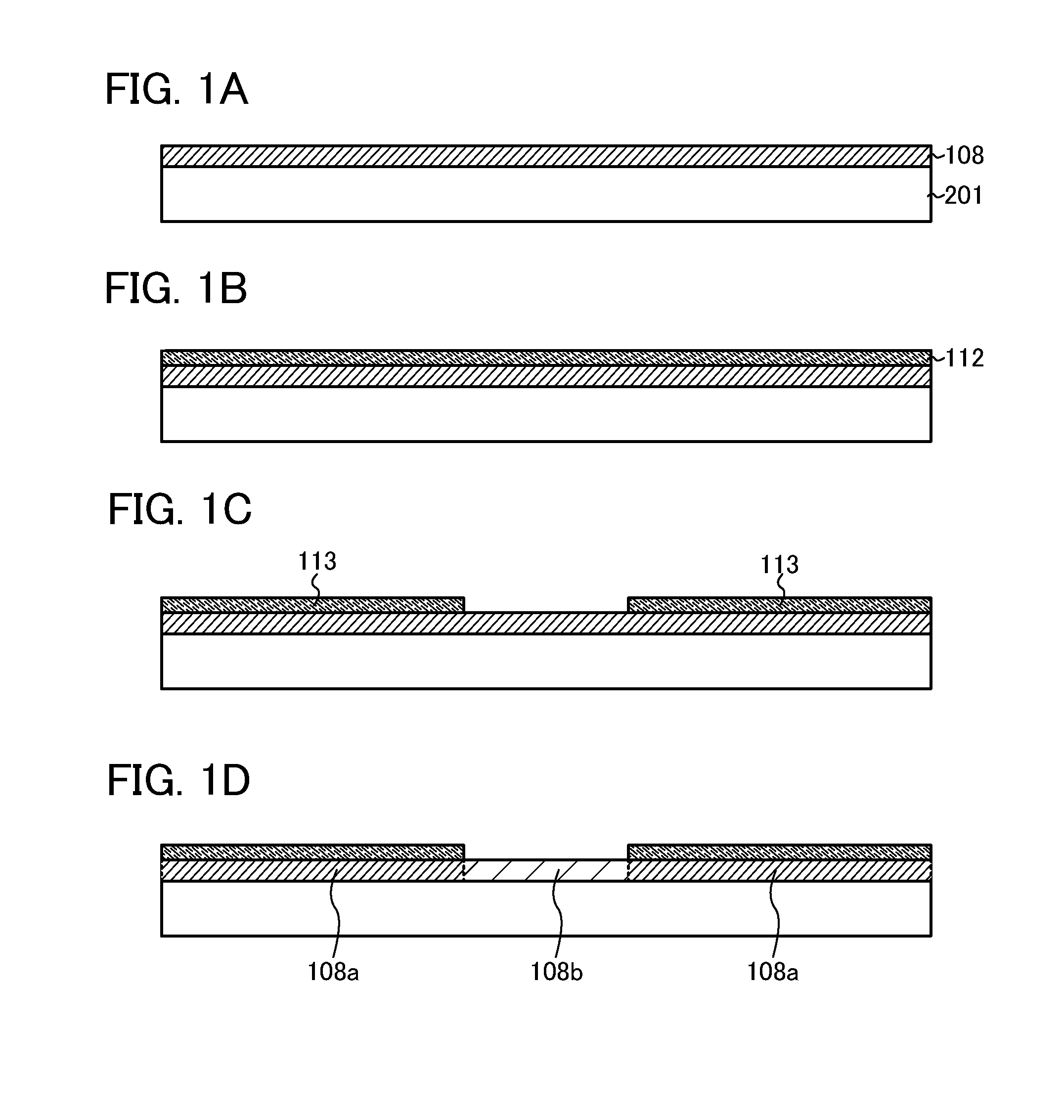
[0062]First, an oxide semiconductor layer 108 including hydrogen is formed over a substrate 201 (see FIG. 1A).

[0063]The oxide semiconductor layer 108 can be formed using a material of which electric resistance is lowered by addition of hydrogen or deuterium. For example, the oxide semiconductor layer 108 can be formed using an oxide semiconductor including at least indium, zinc, gallium, and hydrogen. In this case, deposition is performed by a sputtering method using an oxide semiconductor target including In, Ga, and Zn (for example, In2O3:Ga2O3:ZnO=1:1:1) while a hydrogen gas is introduced, so that the oxide semiconductor layer 108 including hydrogen can be formed.

[0064]The oxide semiconductor layer 108 is formed while hydrogen is introduced into a deposition atmosphere, so that hydrogen can be uniformly added into the oxide semiconductor layer 108 even when the ...

embodiment 2

[0091]In this embodiment, an example of a method for manufacturing a bottom-gate transistor which is described in Embodiment 1 is described with reference to drawings.

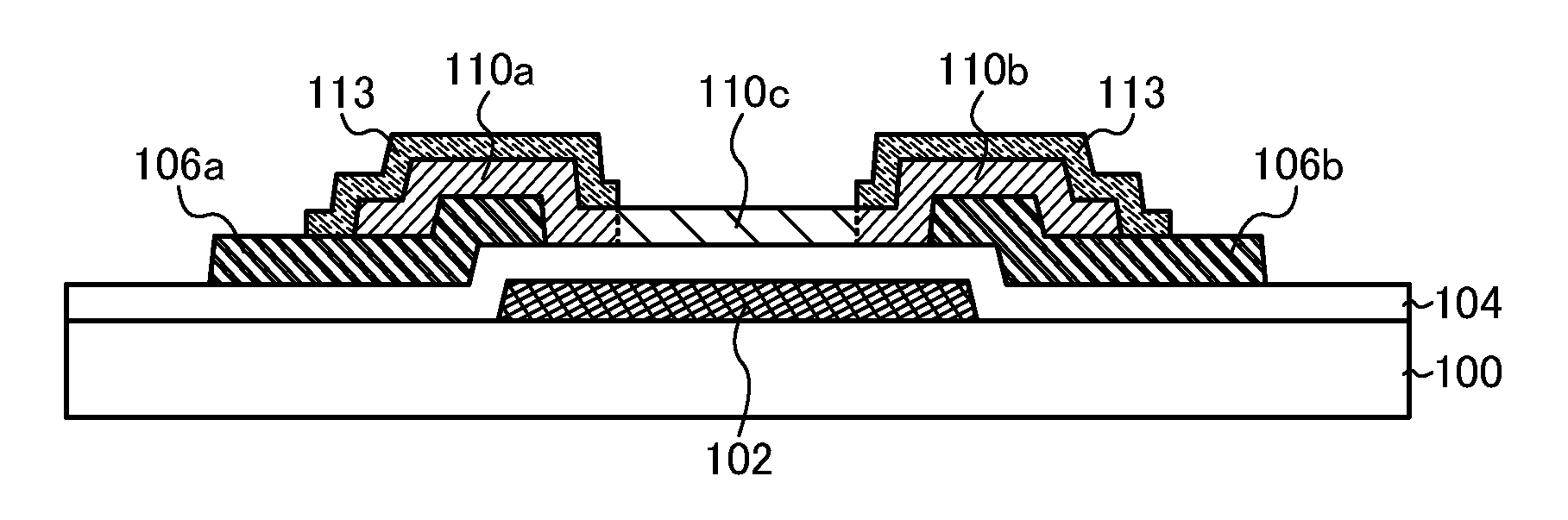
[0092]First, a gate electrode 102 is formed over the substrate 100 and then a gate insulating layer 104 is formed over the gate electrode 102. After that, a source electrode layer 106a and a drain electrode layer 106b are formed over the gate insulating layer 104 (see FIG. 3A).

[0093]The substrate 100 may be any substrate as long as it is a substrate having an insulating surface. A glass substrate can be used, for example. Alternatively, as the substrate 100, an insulating substrate which is formed using an insulator such as a ceramic substrate, a quartz substrate, and a sapphire substrate; a semiconductor substrate which is formed using a semiconductor material such as silicon and whose surface is covered with an insulating material; and a conductive substrate which is formed using a conductor such as metal or stainles...

embodiment 3

[0127]In this embodiment, an example of a method for manufacturing a bottom-gate transistor, which is different from the manufacturing method described in Embodiment 2, is described with reference to drawings.

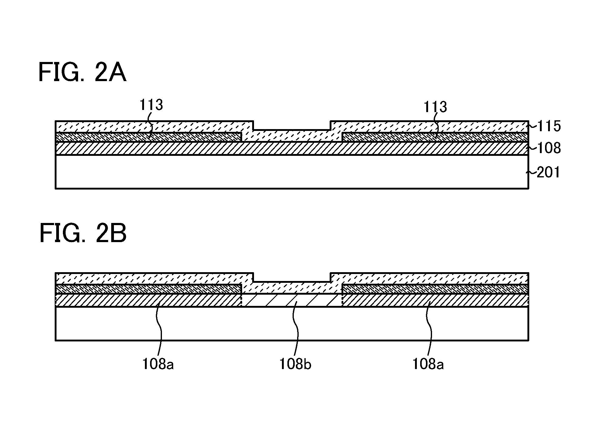
[0128]First, the gate electrode 102 is formed over the substrate 100 and then the gate insulating layer 104 is formed over the gate electrode 102. After that, the oxide semiconductor layer 108 is formed over the gate insulating layer 104 (see FIG. 6A).

[0129]Next, after the oxide semiconductor layer 108 is etched to form the island-shaped oxide semiconductor layer 110 (see FIG. 6B), the hydrogen barrier layer 112 is formed over the oxide semiconductor layer 110 (see FIG. 6C).

[0130]Next, the hydrogen barrier layer 112 is etched so that parts of the hydrogen barrier layer 112 (the hydrogen barrier layers 113) are left and a surface of part of the oxide semiconductor layer 110, which is formed over the gate electrode 102, is exposed (see FIG. 6D).

[0131]Next, hydrogen is desorbed fr...


PUM


Abstract

A hydrogen barrier layer is selectively provided over an oxide semiconductor layer including hydrogen and hydrogen is selectively desorbed from a given region in the oxide semiconductor layer by conducting oxidation treatment, so that regions with different conductivities are formed in the oxide semiconductor layer. After that, a channel formation region, a source region, and a drain region can be formed with the use of the regions with different conductivities formed in the oxide semiconductor layer.

Description

TECHNICAL FIELD[0001]The present invention relates to a method for manufacturing a transistor using an oxide semiconductor layer, and also relates to a method for manufacturing a semiconductor device including the transistor.BACKGROUND ART[0002]Various metal oxides are used for a variety of applications. Indium oxide is a well-known material and is used as a transparent electrode material which is necessary for liquid crystal displays and the like.[0003]Some metal oxides have semiconductor characteristics. Metal oxides having semiconductor characteristics are a kind of compound semiconductor. The compound semiconductor is a semiconductor formed using two or more kinds of atoms bonded together. In general, metal oxides become insulators. However, it is known that metal oxides become semiconductors depending on the combination of elements included in the metal oxides.[0004]For example, it is known that tungsten oxide, tin oxide, indium oxide, zinc oxide, and the like are metal oxides ...

Claims


Application Information

Patent Timeline
Patent Type & Authority Applications(United States)
IPC IPC(8): H01L21/34H05B44/00
CPCH01L21/02554H01L21/02565H01L21/02631H01L22/12H01L29/7869H01L29/66969H01L21/02664H01L27/1225H01L29/41733H01L29/78618H01L29/66742H01L29/78696
Inventor SAKATA, JUNICHIRO
Owner SEMICON ENERGY LAB CO LTD
Why Eureka
Try Eureka