Fabrication method of electronic devices based on aligned high aspect ratio nanoparticle networks

a nanoparticle network and nanoparticle technology, applied in nanoinformatics, natural mineral layered products, cellulosic plastic layered products, etc., can solve the problems of increasing the difficulty of silicon-based electronics, limited performance of organic electronic devices, and a large amount of challenges in the field of nanoparticle network fabrication

Active Publication Date: 2010-07-01
LYTEN INC
View PDF7 Cites 14 Cited by
  • Summary
  • Abstract
  • Description
  • Claims
  • Application Information

AI Technical Summary

Benefits of technology

[0031]The above device structure may further comprise an insulating layer, covering the first and the second conductive terminals and the plurality of high aspect ratio nanoparticles connecting the first and the second conductive terminals, and a third conductive terminal, disposed overlapping the plurality of high aspect ra

Problems solved by technology

However, the silicon-based electronics are facing increasing amount of challenges in both low-end and high-end market segments.
Currently, performance of the organic electronic devices is limited by very low mobility of charge carriers in the organic materials.
This means the fabrication of radio frequency (RF) circuitries or fast display devices remains a challenge.
To the date, industrial scale processes for mass fabrication of single CNT based electronic circuits are not well established.
Besides, because of the limited current-carrying capacity of individual CNT, multiple CNTs aligned side by s

Method used


Image

  • Fabrication method of electronic devices based on aligned high aspect ratio nanoparticle networks
  • Fabrication method of electronic devices based on aligned high aspect ratio nanoparticle networks
  • Fabrication method of electronic devices based on aligned high aspect ratio nanoparticle networks

Examples


Embodiment Construction

[0048]In the following, the principle of the invention is explained through various examples. It is understood that the scope of the present invention is not limited by these particular examples.

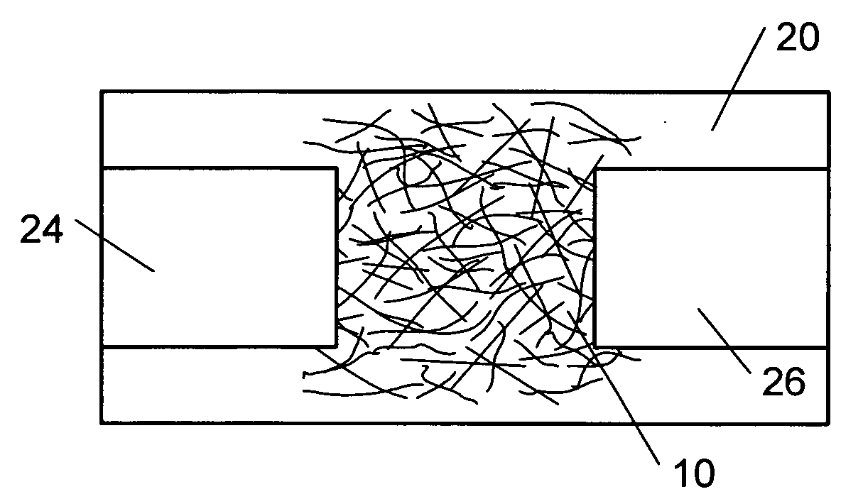
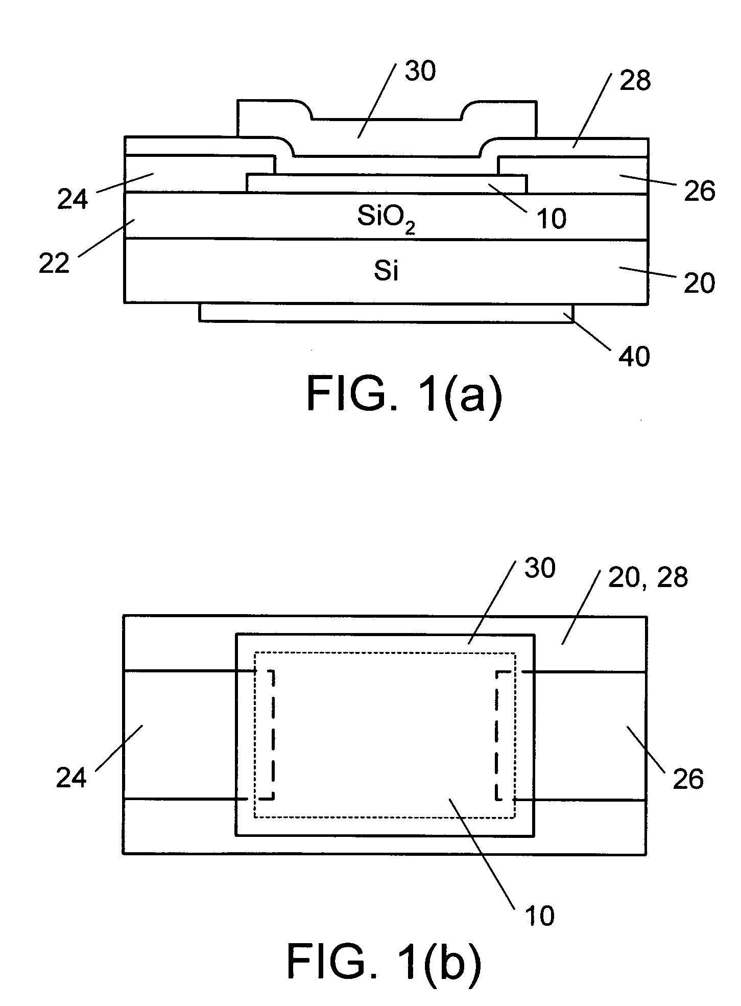
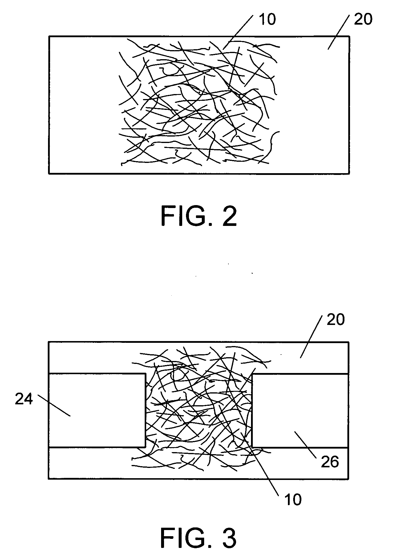
[0049]An exemplary structure of a top gate FET is shown in FIGS. 1(a) and 1(b). A network of semiconducting high aspect ratio nanoparticles (such as carbon nanotubes in individual or bundled form, or carbon nanowires, in particular, SWNTs are preferred) 10 is disposed on a substrate 20 having an insulating top layer 22 (such as a silicon substrate having a silicon dioxide (SiO2) top layer). Two metal contacts 24 and 26 are disposed on the substrate 20, connecting via the CNTN 10. An insulator layer 28 is disposed on the CNTN 10 and the metal contacts 24 and 26. A third metal contact 30 is disposed on the insulator layer 28 above the CNTN 10. The CNTN 10 forms a channel between the two metal contacts 24 and 26 that act as a source terminal and a drain terminal, respectively, and the third met...


PUM

PropertyMeasurementUnit
Fractionaaaaaaaaaa
Electric potential / voltageaaaaaaaaaa
Aspect ratioaaaaaaaaaa

Abstract

A layer of high aspect ratio nanoparticles is disposed on a surface of a substrate under the influence of an electrical field applied on the substrate. To create the electrical field, a voltage is applied between a pair of electrodes arranged near the substrate or on the substrate, and the high aspect ratio nanoparticles disposed on the substrate are at least partially aligned along direction(s) of the applied electrical field. The high aspect ratio nanoparticles are grown from catalyst nanoparticles in an aerosol, and the aerosol is directly used for forming the nanoparticle layer on the substrate at room temperature. The nanoparticles may be carbon nanotubes, in particular single wall carbon nanotubes. The substrate with the layer of aligned high aspect ratio nanoparticles disposed thereon can be used for fabricating nanoelectronic devices.

Description

TECHNICAL FIELD[0001]This disclosure relates to nanostructured materials and their applications in microelectronic devices. In particular, this disclosure relates to a low cost process for making aligned structure of high aspect ratio nanoparticles and using the aligned structure of the high aspect ratio nanoparticles in fabricating the microelectronic devices.BACKGROUND ART[0002]Silicon-based complementary metal-oxide-semiconductor (CMOS) electronics have undergone remarkable progresses over the past 40-50 years. It is expected that, with new materials and device structures continuously being introduced for boosting the performance and reducing the cost, the CMOS electronics will continue to be the workhorse of the information technologies.[0003]However, the silicon-based electronics are facing increasing amount of challenges in both low-end and high-end market segments.[0004]In the low cost segment of the market, organic electronics have made tremendous progress over the last deca...

Claims


Application Information

Patent Timeline
IPC IPC(8): H01L29/66B01J19/08B32B9/00B32B5/16
CPCB82Y10/00B82Y30/00H01L51/0012H01L51/0048H01L51/0545Y10S977/742Y10S977/891B82Y40/00Y10T428/30Y10T428/2991H10K71/191H10K85/221H10K10/466
Inventor ERMOLOV, VLADIMIR ALEXSANDROVICH
Owner LYTEN INC
Why Eureka
Try Eureka