

Optical element, display device, and optical device
a technology of optical elements and display devices, applied in the field of optical elements, display devices, optical devices, can solve the problems of retardation film thickness as a whole, light leakage in a skew direction, yield ratio drops, etc., and achieve the effect of easy control of wavelength dispersion of retardation
- Summary
- Abstract
- Description
- Claims
- Application Information
AI Technical Summary
Benefits of technology
Problems solved by technology
Method used
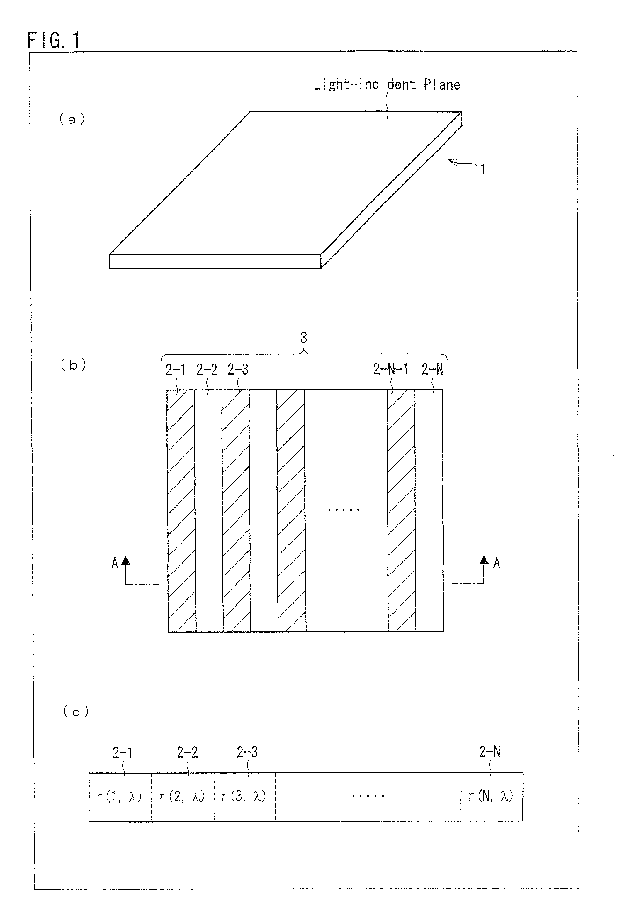
Image

Examples
application example
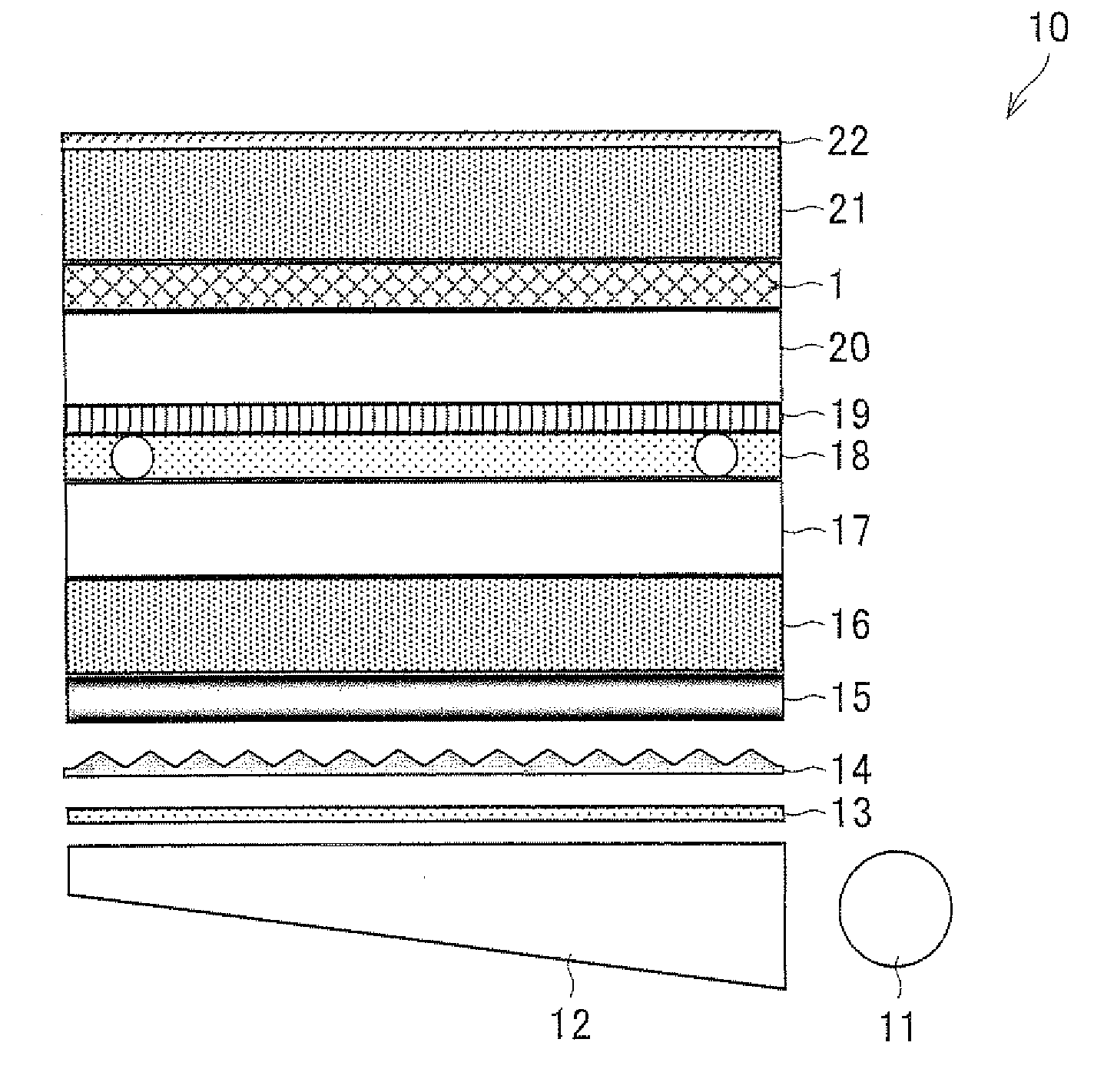
[0229]The retardation film of the present Embodiment is applicable to display devices such as liquid crystal displays and EL displays.
[0230]With the retardation film of the present Embodiment, by suitably selecting retardations and area ratios of unit areas, it is possible to cause synthetic retardation of a whole area to have reverse wavelength dispersion. This allows realizing a retardation film that exhibits reverse wavelength dispersion which is more inclined than wavelength dispersion controlled by a material. Therefore, the retardation film of the present Embodiment is useful for the purpose of preventing reflection in EL displays and liquid crystal displays.
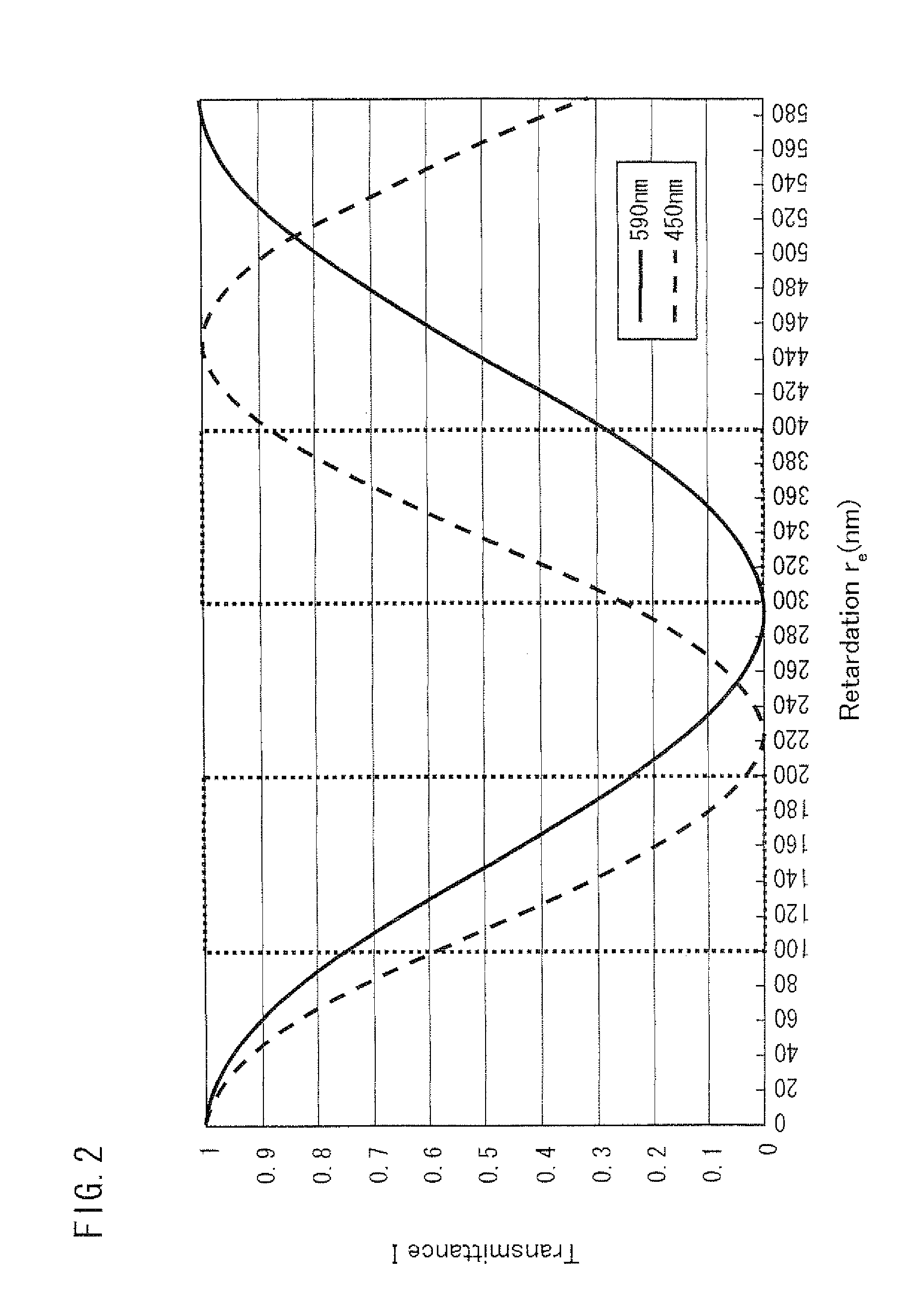
[0231]Further, in a case of optically compensating birefringence of liquid crystal molecules, a retardation film exhibiting the same wavelength dispersion as that of birefringence of the liquid crystal molecules is desirable. With the retardation film of the present Embodiment, by suitably selecting retardations and area r...
PUM
| Property | Measurement | Unit |
|---|---|---|
| wavelength | aaaaa | aaaaa |
| angle | aaaaa | aaaaa |
| width | aaaaa | aaaaa |
Abstract
Description
Claims
Application Information