

Eda tool, semiconductor device, and scan chain configuration method
a technology of scan chain and configuration method, applied in the direction of logical operation testing, instruments, measurement devices, etc., can solve the problems of inability to control the value obtained after ffs receives a response pattern, and so as to reduce the time and man-hour required, and reduce the drop of ir during a scan test
- Summary
- Abstract
- Description
- Claims
- Application Information
AI Technical Summary
Benefits of technology
Problems solved by technology
Method used
Image

Examples
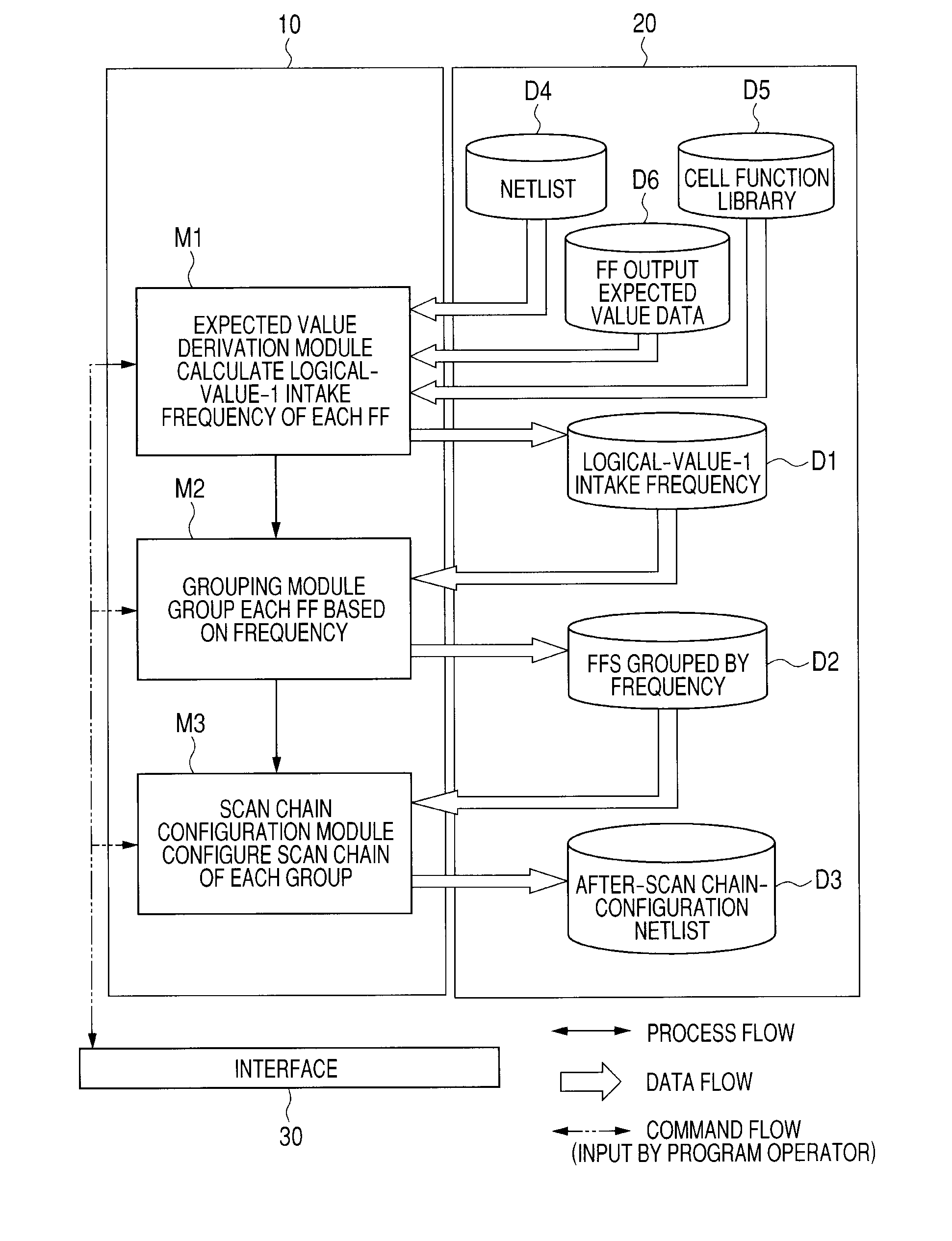
first embodiment
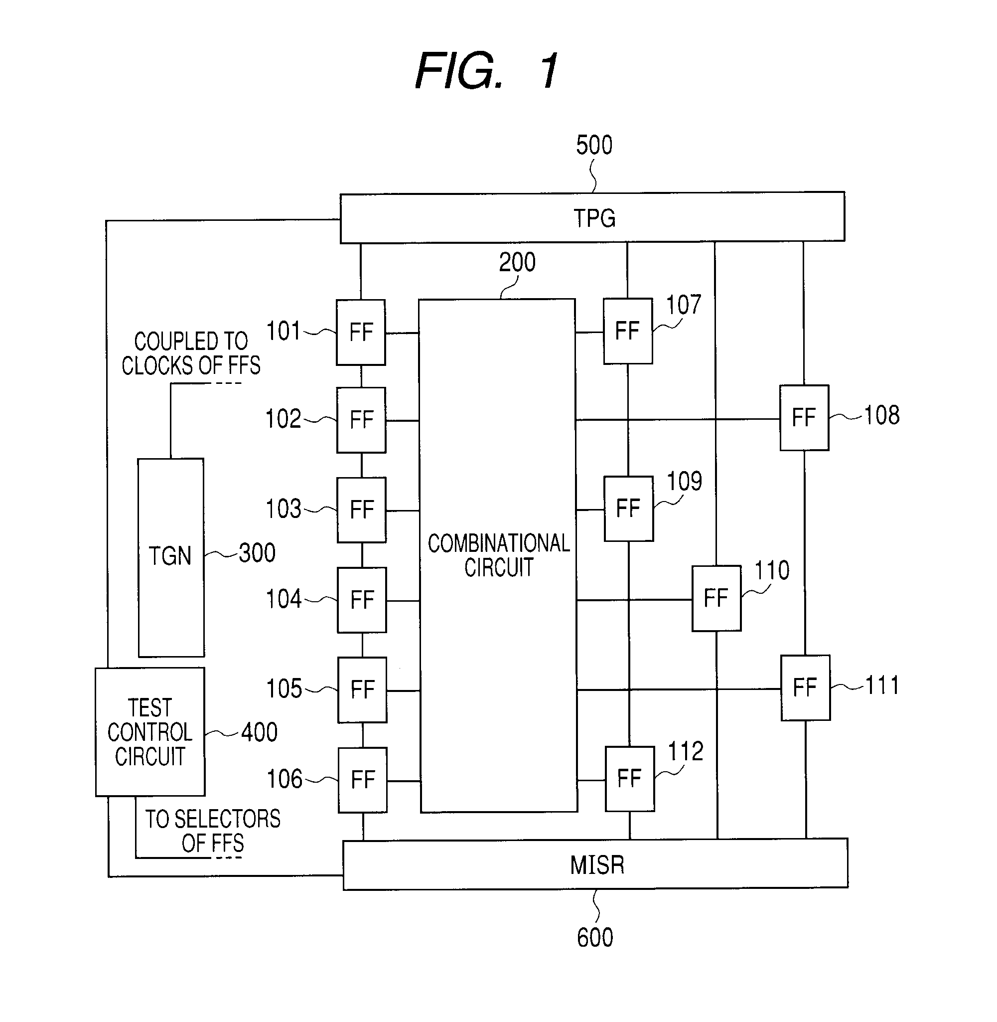
[0034]FIG. 1 is an example of a test circuit and a semiconductor device subject to a scan test with a test pattern according to the present invention.
[0035]The semiconductor device in FIG. 1 includes flip-flops (FFs) 101 to 112, a combinational circuit 200, a test clock generating circuit (TGN) 300, a test control circuit 400, a random-number pattern generating circuit (TPG) 500, and a compression circuit (MISR) 600.
[0036]The FFs 101 to 112 are flip-flop groups for enabling a scan test.
[0037]The combinational circuit 200 is a circuit comprised of a plurality of logic elements. The FFs 101 to 112 are coupled in series so that a test pattern can be applied to the FFs 101 to 112 through external terminals. The coupling of FFs is called a scan chain. In FIG. 1, the FFs 101 to 106 configure a scan chain, the three FFs 107, 109, and 112 configure another scan chain, the two FFs 108 and 111 configure another scan chain, and only the FF 110 configures the other scan chain.
[0038]The test clo...
second embodiment
[0105]Next, the second embodiment of the invention will be described.
[0106]In the first embodiment, probability propagation is derived by calculation to obtain the frequency of intake of the logical value “1”. In the second embodiment, a method for obtaining the frequency by performing logic simulation will be explained. The configuration diagram of the EDA tool according to the invention is substantially the same as FIG. 4, and therefore is omitted herein. In this embodiment, the FF output expected value data D6 is not used.
[0107]FIG. 8 is a flowchart showing a procedure for expected value derivation according to the second embodiment of the invention. This process is substituted for that of FIG. 5. Accordingly, assume that the EDA tool body which operates in the execution unit 10 has already read the expected value derivation module M1 from the data storage unit 20 and started the execution before the start of the process of FIG. 8. Further, assume that readout from the netlist D4...
PUM
 Abstract
Description
Claims
Application Information