Electronic device test apparatus and method of testing electronic devices

Inactive Publication Date: 2010-06-17
ADVANTEST CORP
View PDF12 Cites 7 Cited by
  • Summary
  • Abstract
  • Description
  • Claims
  • Application Information

AI Technical Summary

Benefits of technology

[0007]The present invention has as its object the provision of an electronic device test apparatus easily removing ICs unsuitably held on a test tray and able to prevent damage to a test tray and ICs.
[0009]In the present invention, a posture of the test tray is changed in a direction dropping devices under test at least once before testing the devices under test. Due to this, it is possible to drop the ICs unsuitably held on the test tray and easily remove the electronic devices before testing, so it is possible to prevent damage to the test tray and the devices under test.
[0035]In the present invention, a posture of the test tray is changed in a direction dropping devices under test at least once before testing the devices under test. Due to this, it is possible to drop devices under test unsuitably held on a test tray and easily remove such electronic devices before testing, so it is possible to suppress breakage of the test tray and devices under test.

Problems solved by technology

If a test tray with ICs unsuitably held is conveyed to the test head to be tested, when pushing the ICs against the contact parts of the test head, the test tray, contact parts, pushers for pushing the ICs, or ICs themselves are liable to be damaged.
However, since the test tray holds a large number of (for example 64 or 128) ICs, detecting each and every one of these causes increased costs and lower throughput.
This also causes increased costs and lower throughput.

Method used


Image

  • Electronic device test apparatus and method of testing electronic devices
  • Electronic device test apparatus and method of testing electronic devices
  • Electronic device test apparatus and method of testing electronic devices

Examples


first embodiment

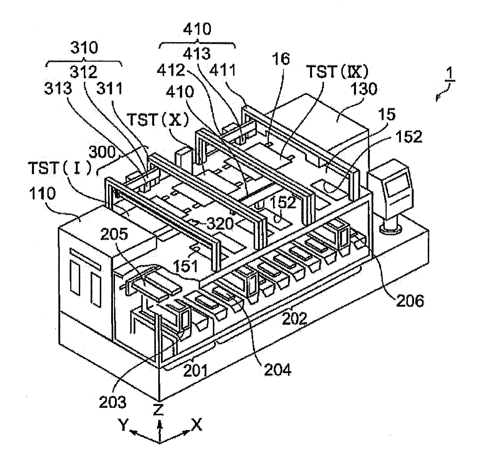
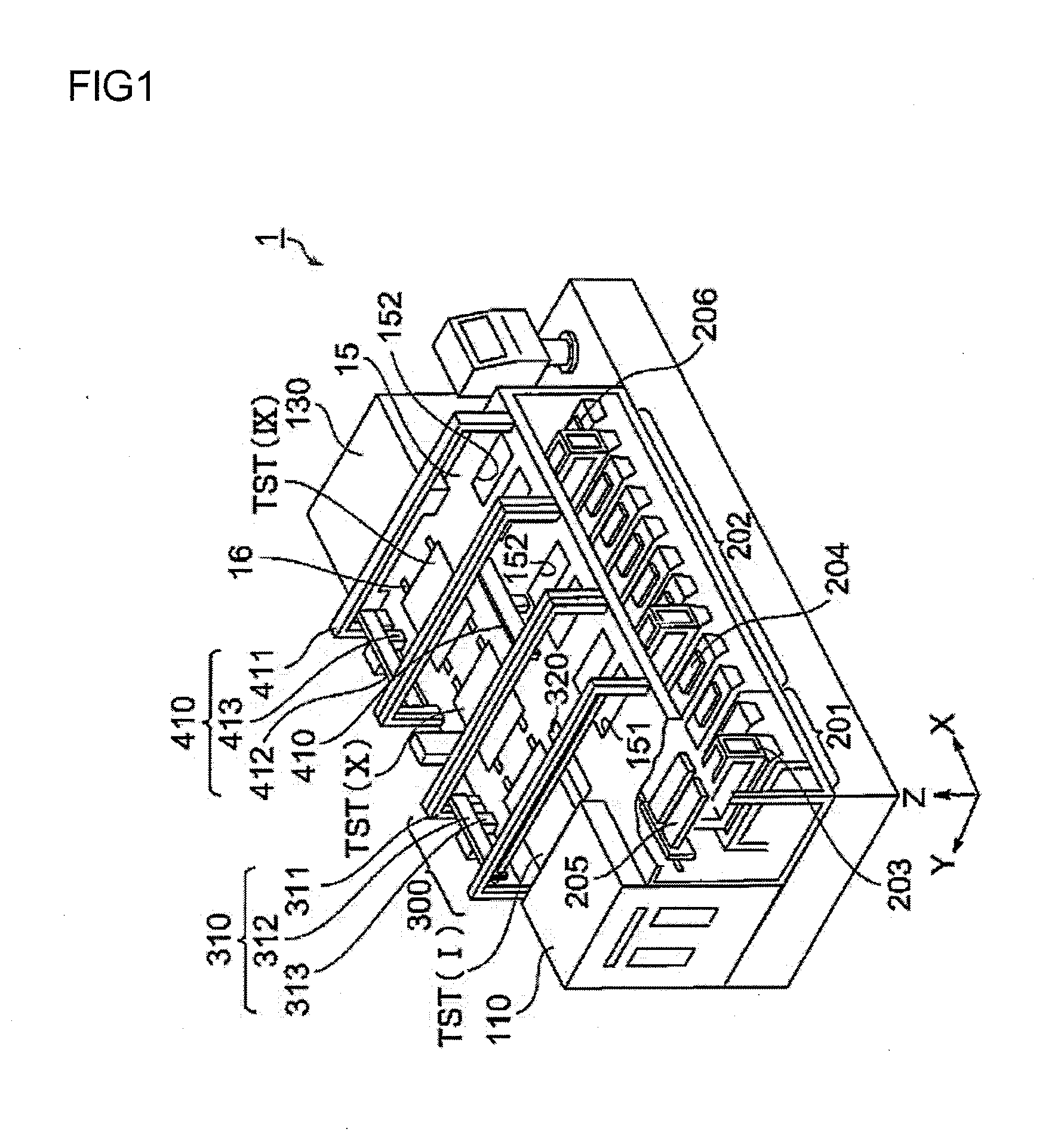
[0098]FIG. 1 is a perspective view of an entire electronic device test apparatus according to the present embodiment, FIG. 2 is a side view showing an electronic device test apparatus according to the present embodiment, FIG. 3 is a conceptual view showing the handling of a tray in an electronic device test apparatus according to the present embodiment, FIG. 4 is a schematic perspective view showing the 3D handling of a test tray in an electronic device test apparatus according to the present embodiment, FIG. 5 is a schematic perspective view showing the handling of the test tray along the vertical direction in a soak chamber of an electronic device test apparatus according to the present embodiment, FIG. 6 is a schematic perspective view showing the handling of the test tray along the vertical direction in an unsoak chamber of an electronic device test apparatus according to the present embodiment.

[0099]The electronic device test apparatus according to the present embodiment , as s...

second embodiment

[0156]FIG. 17 is a perspective view showing an entire electronic device test apparatus according to the present embodiment, FIG. 18 is a schematic cross-sectional view along the line XVIII-XVIII of FIG. 17, FIG. 19 is a conceptual view showing the handling of a tray in an electronic device test apparatus according to the present embodiment, FIG. 20 is a schematic perspective view showing the 3D handling of a test tray in an electronic device test apparatus according to the present embodiment, and FIG. 21 and FIG. 22 are a front view and side view showing an inversion system and a collection system of an electronic device test apparatus according to the present embodiment.

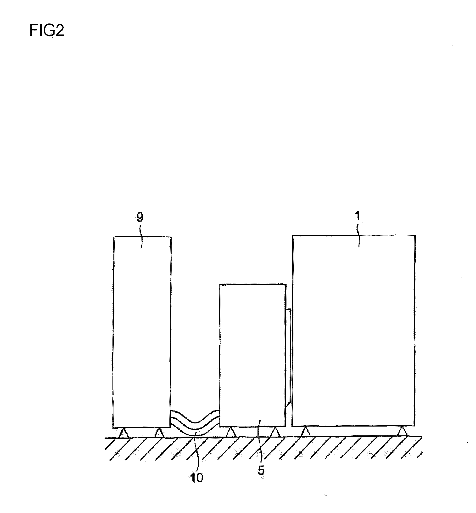
[0157]The electronic device test apparatus according to the present embodiment, as shown in FIG. 17 to FIG. 19, comprises a handler 1, test head 5, and tester 9. Its basic configuration is the same as that of the electronic device test apparatus according to the first embodiment.

[0158]However, the electronic device ...


PUM


Abstract

An electronic device test apparatus used for bringing the ICs into electrical contact with contact parts of the test head in the state where the ICs are held on a test tray and running tests on the electrical characteristics of ICs, the electronic device test apparatus including an inversion system for rotating the test tray which holds a plurality of ICs in a direction dropping ICs which are insufficiently held at least once before testing.

Description

TECHNICAL FIELD[0001]The present invention relates to an electronic device test apparatus for testing semiconductor integrated circuit chips or other electronic devices (hereinafter referred to representatively as “IC devices”).BACKGROUND ART[0002]In the process of production of IC devices and other electronic devices, an electronic device test apparatus is used for testing IC devices for performance or functions in a packaged state.[0003]A handler, forming part of an electronic device test apparatus, reloads a large number of IC devices from a customer tray to a test tray, conveys the test tray inside the handler, brings the IC devices into electrical contact with the contact parts of a test head in the state held on the test tray, and the main body of the electronic device test apparatus (hereinafter also referred to as a “tester”) executes a test. Further, after the test ends, the test tray holding the IC devices is carried out from the test head and the devices are reloaded on c...

Claims


Application Information

Patent Timeline
IPC IPC(8): G01N1/00G01R31/02
CPCG01R31/2893
Inventor ITO, AKIHIKOKARINO, KOYAKOBAYASHI, YOSHIHITO
Owner ADVANTEST CORP
Why Eureka
Try Eureka