Ring buffer circuit and control circuit for ring buffer circuit

a control circuit and buffer circuit technology, applied in the field of ring buffer circuits, can solve problems such as the inability to avoid erroneous operation

Active Publication Date: 2010-07-08
RENESAS ELECTRONICS CORP
View PDF21 Cites 31 Cited by
  • Summary
  • Abstract
  • Description
  • Claims
  • Application Information

AI Technical Summary

Benefits of technology

[0015]Further, according to another aspect of the present invention, a control circuit for a ring buffer circuit having addresses specified by N bits (N is an integer equal to or larger than two) includes: a read address counter pointer for designating a read address of the ring buffer circuit; a write address counter pointer for designating a write address of the ring buffer circuit; and a comparison operation section for comparing the read address and the write address to detect whether or not the ring buffer circuit is empty and whether or not the ring buffer circuit is full, in which the read address counter pointer and the write

Problems solved by technology

Therefore, even in a case where the write pointer (WP) and the read pointer (RP) are gray-encoded, when the additiona

Method used


Image

  • Ring buffer circuit and control circuit for ring buffer circuit
  • Ring buffer circuit and control circuit for ring buffer circuit
  • Ring buffer circuit and control circuit for ring buffer circuit

Examples


embodiment 1

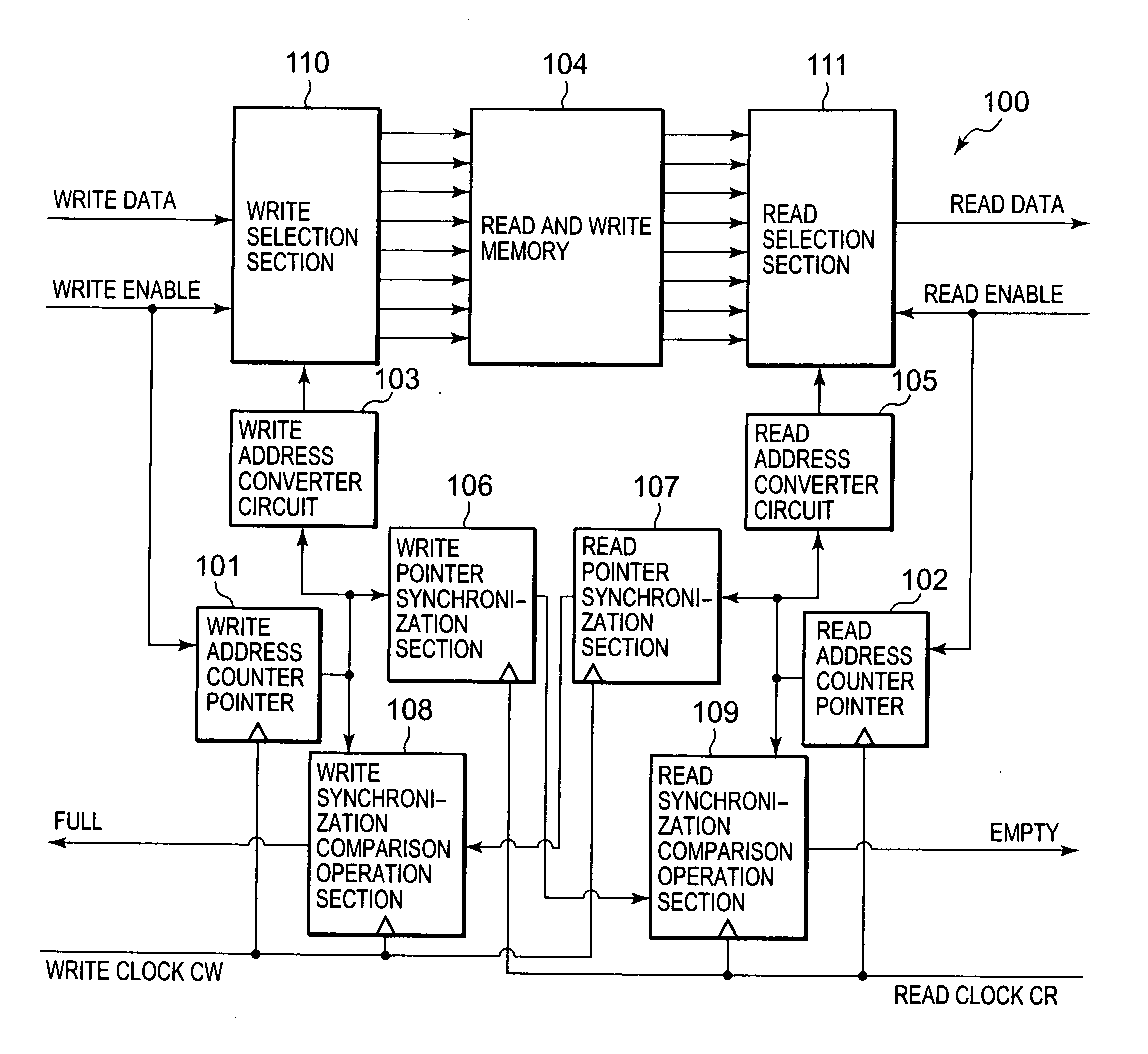
[0045]FIG. 1 is a block diagram illustrating the structure of the ring buffer circuit according to Embodiment 1. In FIG. 1, the ring buffer circuit includes: the dual port memory having the write selection section 110 and the read selection section 111 which respectively serve as the write port and read port of the read and write memory 104; and the control circuit for causing the dual port memory to serve as the ring buffer. The control circuit for the ring buffer principally includes the write address counter pointer 101, the read address counter pointer 102, the write address converter circuit 103, the read address converter circuit 105, the write pointer synchronization section 106, the read pointer synchronization section 107, the write synchronization comparison operation section 108, and the read synchronization comparison operation section 109.

[0046]The write selection section 110 writes data into an address of the read and write memory 104 which is indicated by the write ad...

embodiment 2

[0066]When the same clock is used for the write clock CW and the read clock CR, Embodiment 1 may be applied to the ring buffer in which the write operation and the read operation are synchronous with each other. However, when it is known in advance that the write operation and the read operation are synchronous with each other, the circuit according to Embodiment 1 may be further simplified.

[0067]FIG. 6 is a block diagram illustrating the entire ring buffer circuit according to Embodiment 2. In FIG. 6, Embodiment 2 is different from Embodiment 1 in that a common clock is used for writing and reading, the write pointer synchronization section and the read pointer synchronization section are omitted, and a″ single comparison operation section 112 for generating the internal state signals is provided. The other structure and operation are substantially the same as Embodiment 1. Therefore, the same reference numerals as in Embodiment 1 are used and the detailed description thereof is om...

embodiment 3

[0071]When a clock synchronous with the write clock CW and the read clock CR is used, the ring buffer circuit according to Embodiment 1 described above may be applied to the ring buffer circuit in which the write operation and the read operation are synchronous with each other. However, in the case where the write clock and the read clock are synchronous with each other, when the write pointer synchronization section 106 or the read pointer synchronization section 107 is bypassed, the ring buffer circuit may be operated at higher speed.

[0072]FIG. 7 is a block diagram illustrating the entire structure of a ring buffer circuit according to Embodiment 3. The ring buffer circuit according to Embodiment 3 is different from the ring buffer circuit according to Embodiment 1 as illustrated in FIG. 1 in that a write pointer selection section 113 and a read pointer selection section 114 are further provided and the write pointer selection section 113 and the read pointer selection section 114...


PUM


Abstract

Provided are a ring buffer circuit in which a data full state and a data empty state may be correctly detected without depending on whether read and write operations are synchronous or asynchronous with each other, and a control circuit for the ring buffer circuit. The ring buffer circuit includes: a read and write memory having addresses specified by N bits; a write address counter pointer and a read address counter pointer which are provided for the read and write memory to count (N+1)-bit gray codes; and write and read address converter circuits provided to convert the (N+1)-bit gray codes output from the write and read address counter pointers into N-bit addresses which may be directly designated as write and read addresses of the read and write memory.

Description

BACKGROUND OF, THE INVENTION[0001]1. Field of the Invention[0002]The present invention relates to a ring buffer circuit in which pointers may be circulated within a predetermined address area to perform read and write operations, and to a control circuit for the ring buffer circuit. In particular, the present invention relates to a ring buffer circuit in which read and write operations may be asynchronously performed using a dual port memory, and to a control circuit for the ring buffer circuit.[0003]2. Description of the Related Art[0004]It is generally important for a first-in first-out (FIFO) type data buffer device (hereinafter, referred to as FIFO buffer) to output a signal indicating an internal state to an external circuit (hereinafter, referred to as internal state signal), to prevent writing in a state in which a storage region is full (hereinafter, referred to as full state) or reading in an empty state in which the reading of all write data from the storage region is comp...

Claims


Application Information

Patent Timeline
IPC IPC(8): G06F12/00
CPCG06F5/14G06F2205/106G06F2205/102
Inventor YAGIHASHI, KIYOTO
Owner RENESAS ELECTRONICS CORP
Why Eureka
Try Eureka