Probe Card

a technology of probes and probes, applied in the field of probe cards, can solve problems such as reducing the efficiency of production and testing, and achieve the effect of raising the accuracy of the test data of the prob

Inactive Publication Date: 2010-07-22
KING YUAN ELECTRONICS
View PDF2 Cites 7 Cited by
  • Summary
  • Abstract
  • Description
  • Claims
  • Application Information

AI Technical Summary

Benefits of technology

[0013]Based on the principle of the current loop, the ground circuit formed cooperatively by the conductive wire and the conductive layer extends to cover a longer range of the probe, such that the loop inductance of the probe in the insulating seat can be reduced and thus the accuracy of the test data of the probe can be raised. The at least a probe may inclu

Problems solved by technology

However, as a conventional probe card of a suspension arm type is applied to the high frequency test, the test result will not be very stable, quite often due to noise produced by electromag

Method used


Image

  • Probe Card
  • Probe Card
  • Probe Card

Examples


Embodiment Construction

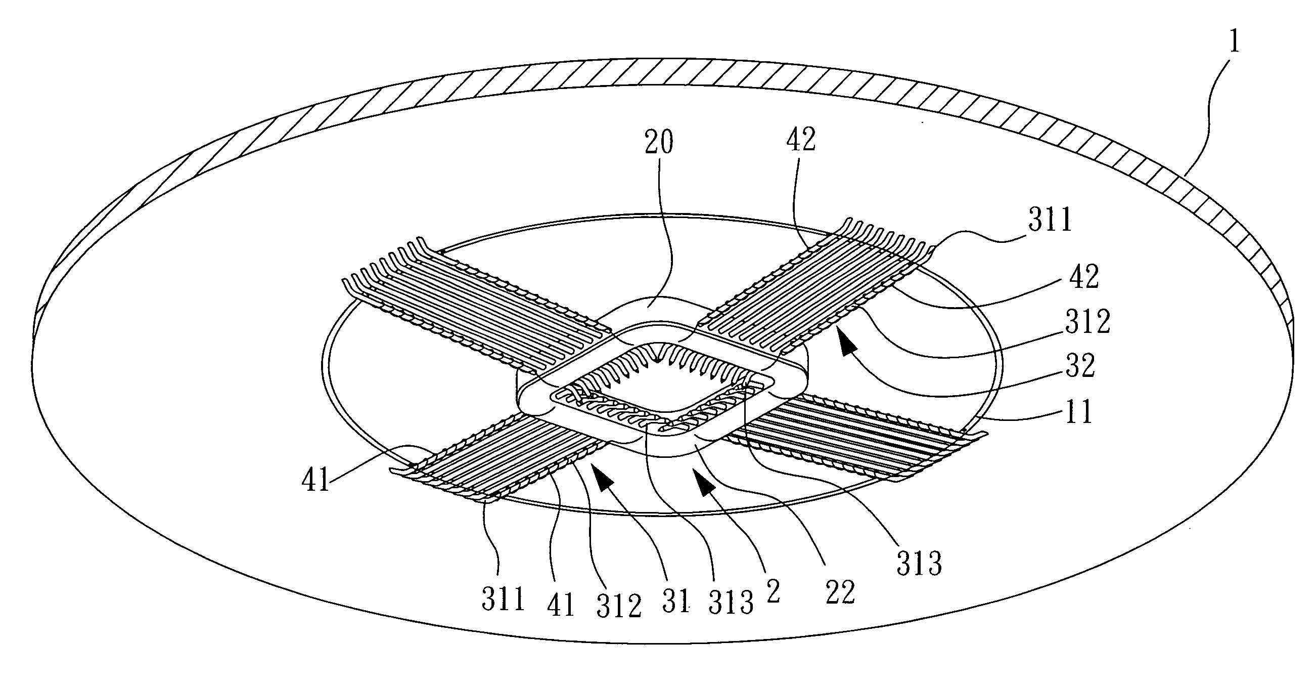
[0020]Please refer to FIG. 3 and FIG. 4 concurrently. FIG. 3 is a three-dimensional diagram of a preferred embodiment of a probe card of the invention. FIG. 4 is a cross-sectional diagram of the preferred embodiment of the probe card of the invention.

[0021]As shown in the drawings, the present invention provides a probe card, comprising a circuit board 1, a probe stand 2, at least a probe 31,32 and at least a conductive wire 41,42.

[0022]The circuit board 1 includes a test circuit 10 and a ground circuit II. The probe stand 2 includes an insulating seat 20, a conductive layer 22 and at least a conductive pin 23, in which one surface of the insulating seat 20 is fixed on a central portion of the circuit board 1 and the other surface thereof is provided with the conductive layer 22. The insulating seat 20 of the probe stand 2 is a hollow body and the conductive layer 22 is a thin layer of a hollow ring. In addition, the insulating seat 20 of the probe stand 2 may be an epoxy seat. The ...


PUM


Abstract

A probe card is disclosed, which has a conductive layer additionally provided on an insulating seat of a probe stand and the conductive layer is electrically connected to a ground circuit on the probe card via a conductive pin being fed through the insulating seat. A conductive wire is wound surrounding the intermediate segment of the probe, one end of the conductive wire is electrically connected to the ground circuit of the circuit board, and the other end of the conductive wire is electrically connected to the conductive layer of the probe stand. Thus, due to that an additional ground portion of the conductive layer is provided on the conductive wire wound surrounding the probe, a loop inductance of the probe in the insulating seat can be reduced such that accuracy of test data of the probe can be enhanced.

Description

BACKGROUND OF THE INVENTION[0001]1. Field of the Invention[0002]The present invention relates to a probe card and, more particularly, to a probe card having a conductive layer.[0003]2. Background of the Invention[0004]In processing wafers of semiconductor, to determine if dies on a wafer are good or bad, a test bench and a probe card are required to perform test of the wafer. It is provided on the probe card precise a contact mechanism to contact each die on the wafer and a conduction circuit to perform electrical test, so as to assure that the electrical properties and performance of the dies are manufactured according to the design specification.[0005]Recently, development of high speed semiconductor devices is becoming popular. The test bench and the probe card should be operated in high frequency to accommodate the tendency. However, as a conventional probe card of a suspension arm type is applied to the high frequency test, the test result will not be very stable, quite often d...

Claims


Application Information

Patent Timeline
IPC IPC(8): G01R1/067
CPCG01R1/07342G01R1/06772
Inventor NI, CHENG-CHINCHEN, KUN CHOU
Owner KING YUAN ELECTRONICS
Why Eureka
Try Eureka