

Image sensor
a technology of image sensor and image, applied in the field of image sensor, can solve the problems of reducing image quality, complicated blooming phenomenon, and dedicated circuit for providing shutter for avoiding, and achieve the effect of simple configuration and good image quality
- Summary
- Abstract
- Description
- Claims
- Application Information
AI Technical Summary
Benefits of technology
Problems solved by technology
Method used
Image

Examples
Embodiment Construction
[0039]Hereinafter, a specific embodiment to which the present invention is applied will be described in detail with reference to the drawings.
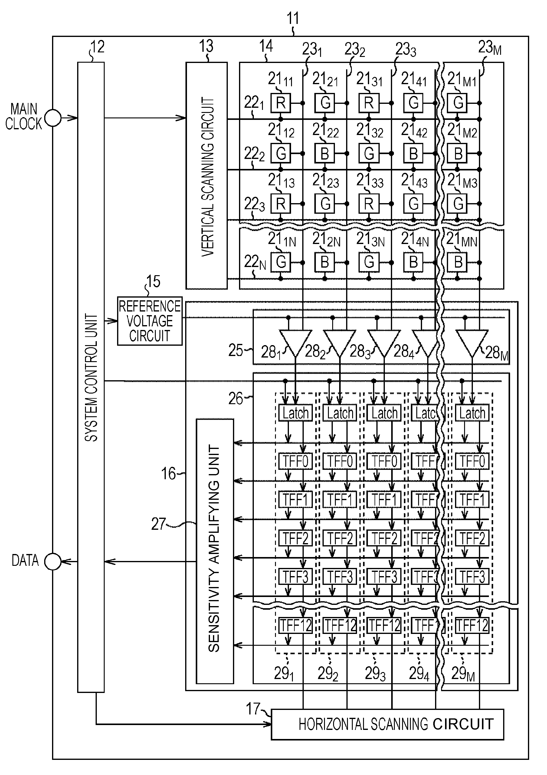
[0040]FIG. 1 is a block diagram illustrating a configuration example of an embodiment of a CMOS sensor to which the present invention is applied.
[0041]In FIG. 1, a CMOS sensor 11 is configured including a system control unit 12, a vertical scanning circuit 13, a pixel array 14, a reference voltage circuit 15, a column ADC (Analog to Digital Converter) 16, and a horizontal scanning circuit 17.
[0042]The system control unit 12 includes a logic control circuit, a PLL circuit (CLK frequency dividing), a timing control circuit, a communication interface, etc. A main clock is supplied to the system control unit 12 from an external circuit that is not illustrated, and the system control circuit 12 performs control of respective blocks constituting the CMOS sensor 11 and communication with the external circuit.
[0043]The vertical scanning circuit 13 seq...
PUM
 Abstract
Description
Claims
Application Information