Photo-sensitive element for electro-optical sensors

a technology of electro-optical sensors and photo-sensitive elements, applied in the field of photo-sensitive elements, can solve the problems of not being able to arbitrarily select one or more, not being able to operate optimally in the presence of light, and not being able to achieve the effect of good immunity and efficient processing

Inactive Publication Date: 2005-05-10
ETH LAB SRL
View PDF12 Cites 2 Cited by
  • Summary
  • Abstract
  • Description
  • Claims
  • Application Information

AI Technical Summary

Benefits of technology

[0016]To be more exact, the purpose of the invention is to obtain an output signal, deriving from the logarithmic conversion of an input signal, of a sufficiently high value to allow an efficient processing and good immunity with respect to the electric no

Problems solved by technology

Previously, such optical sensors were usually made using CCD technology (Charge-Coupled Device), which guarantees a very satisfactory image quality in the presence of a well controlled illumination, but are not able to operate optimally in the presence of a light with an intensity which is greatly differentiated inside the same scene, that is, with an input signal having high dynamics, up to 120 dB.
CCDs are also not very versatile from various points of view: they cannot easily be integrated with complex pilot circuits in a single silicon support or microchip, it is not possible to arbitrarily select one or more pixels inside the matrix sensor and it is possible to acquire the images only after having waited a latency time correlated to the integration time, or exposure, of each pixel to the light.
The logarithmic conversion, obta

Method used


Image

  • Photo-sensitive element for electro-optical sensors
  • Photo-sensitive element for electro-optical sensors
  • Photo-sensitive element for electro-optical sensors

Examples


Embodiment Construction

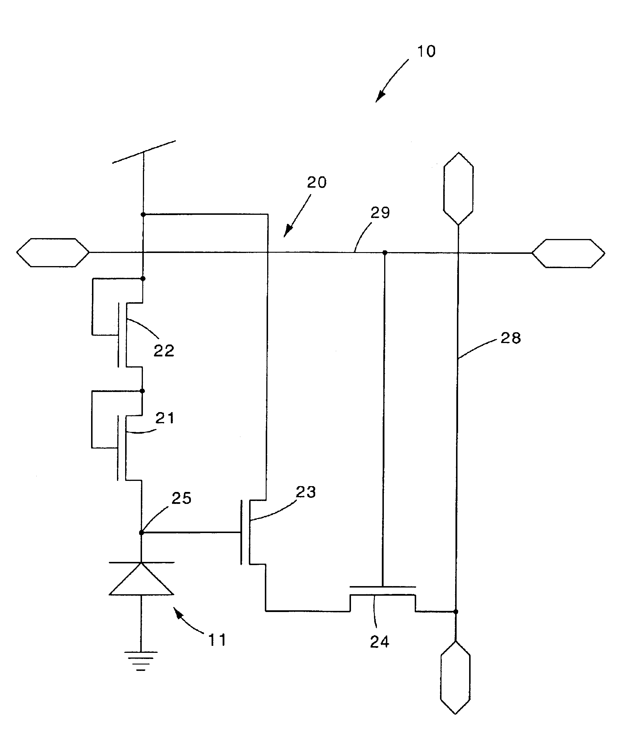
[0031]With reference to the attached drawing of FIG. 1, a photo-sensitive element or pixel 10 according to a first embodiment of the invention consists of an inversely polarized diode 11 of N-type, two transistors of N-type, respectively a first 21 and a second 22, to polarise the photo-diode 11, and an amplification and reading circuit 20 comprising two transistors, respectively third 23 and fourth 24.

[0032]The pixel 10 is of the type able to detect light of a wavelength between 400 and 1000 nm and an intensity which varies in an interval of at least 6 decades, between 10−3 and 10−3 W / m2, and is able to constitute the single cell of a multiple cell matrix sensor made entirely with CMOS technology and hence able to be integrated in a chip.

[0033]The diode 11 is made by a joint between an N type insulated diffusion, medium doped, called Nwell, and the silicon substrate which is weak doped. The interface area between the two parts of the diode is emptied of free loads and characterized...


PUM


Abstract

Photo-sensitive element for electro-optical sensors realised with the CMOS technology, comprising a photo-sensitive reception member (11, 31) consisting of a diode connected to a conversion circuit to convert the current generated by the photo-sensitive reception member (11, 31) into a tension signal, and an amplification and reading circuit (20, 40). The circuit comprises two transistors (21, 22; 41, 42), arranged in a diode configuration with the drain short-circuited with its own gate, the two transistors (21, 22; 41, 42) being connected in series there between and able to perform a logarithmic conversion of the current, photo-generated by the reception member (11, 31), in continuous time and without requiring time to integrate the light. The photo-sensitive element further comprises a third transistor (23, 43) having its gate connected to a photo-sensitive node (25, 45) at an output of the photo-diode (11, 31) to achieve a first stage of amplification in current of the signal by transferring the tension present on the node (25, 45) to the drain of a fourth transistor (24, 44).

Description

FIELD OF THE INVENTION[0001]The present invention concerns a photo-sensitive element, realised with the CMOS technology and used in electro-optical sensors, suitable to detect an incident light and to convert it into a correlated electric signal.[0002]The photo-sensitive element according to the invention is used to make electro-optical sensors of a two-dimensional linear or matrix type which can be used in various electronic devices for artificial vision, such as for example digital video cameras, intelligent optical sensors or otherwise.[0003]The photo-sensitive element according to the invention is particularly suitable for applications which require to detect images in the presence of uncontrolled light, hence characterized by variable intensity over a wide interval, for example to make electro-optical sensors used in the field of automobiles, in security controls, in road safety control and in traffic control.BACKGROUND OF THE INVENTION[0004]The state of the art includes optica...

Claims


Application Information

Patent Timeline
IPC IPC(8): H04N3/15H04N5/355
CPCH04N5/35518H04N3/155H04N25/573
Inventor TECCHIOLLI, GIAMPIETROSARTORI, ALVISE
Owner ETH LAB SRL
Why Eureka
Try Eureka