Programmable resistance memory

a technology of programmable resistance and memory, which is applied in the direction of digital storage, instruments, electrical equipment, etc., can solve the problems of resistance drift, ambiguous programmatic state of the device, and the tendency of the device's resistance to increase over time, so as to increase the memory's dynamic/drift ratio and maximize storage level separation

Inactive Publication Date: 2010-07-22
OVONYX MEMORY TECH LLC
View PDF2 Cites 17 Cited by
  • Summary
  • Abstract
  • Description
  • Claims
  • Application Information

AI Technical Summary

Benefits of technology

[0012]In accordance with the principles of the present invention a high dynamic range alloy may be employed as a memory's programmable resistance material. By employing high dynamic range programmable resistance materials, a memory in accordance with the principles of the present invention may increase the memory's dynamic / drift ratio. In particular, recognizing that, although the composition of a phase change alloy may be a significant factor in the determination of a memory element's drift characteristics, the composition also plays a significant role in determining the resistance dynamic range in programmable resistance devices. In such an embodiment, even with compositions providing no improvement in the memory's resistance drift, because the phase change material exhibits a higher dynamic range, the overall drift-contribution to MLC resistance level change with time is diminished by comparison.
[0013]In accordance with the principles of the present invention, storage levels may be assigned within a device's resistance range in a manner that accommodates variations across an array of devices. Such variations may be due to varying sensitivity to programming currents among the devices, inconsistencies of current programming sources, structural differences among various memory elements, or compositional variations among the devices, for example. Additionally, in an illustrative embodiment, drift at a plurality of storage levels may be factored in to the assignment of resistance values to storage levels in a manner that maximizes storage level separation.

Problems solved by technology

One impediment to wide-spread adoption of the multi-level cell technology is the tendency the devices' resistance to increase over time.
That resistance increase may, over time, render the programmed state of the device ambiguous.
In multi-level cell embodiments, where an individual memory element is programmed to one of three or more resistance values, this phenomenon, generally referred to as, resistance drift, or, simply, drift, is particularly troublesome and a number of drift-compensation techniques have been proposed.

Method used


Image

  • Programmable resistance memory
  • Programmable resistance memory
  • Programmable resistance memory

Examples


Embodiment Construction

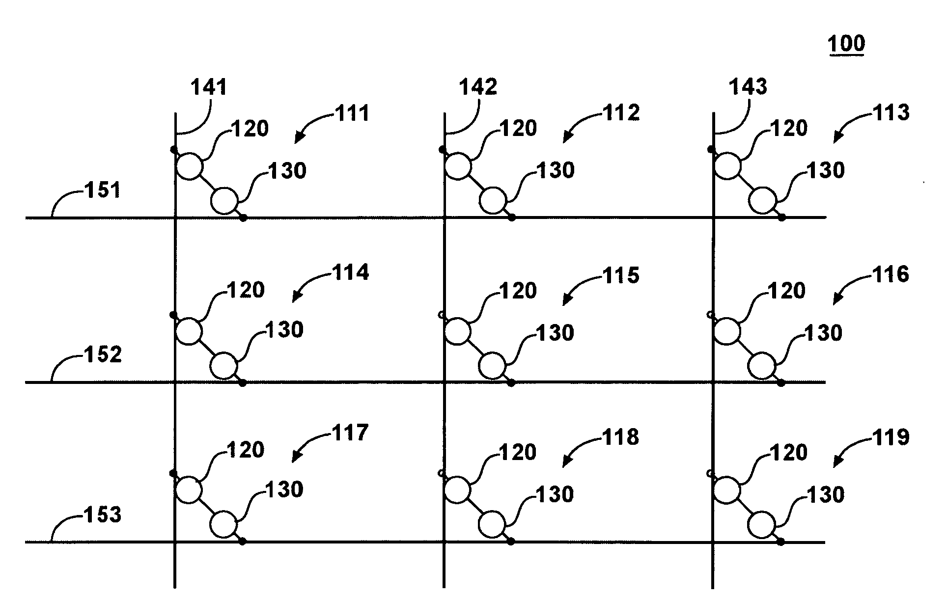
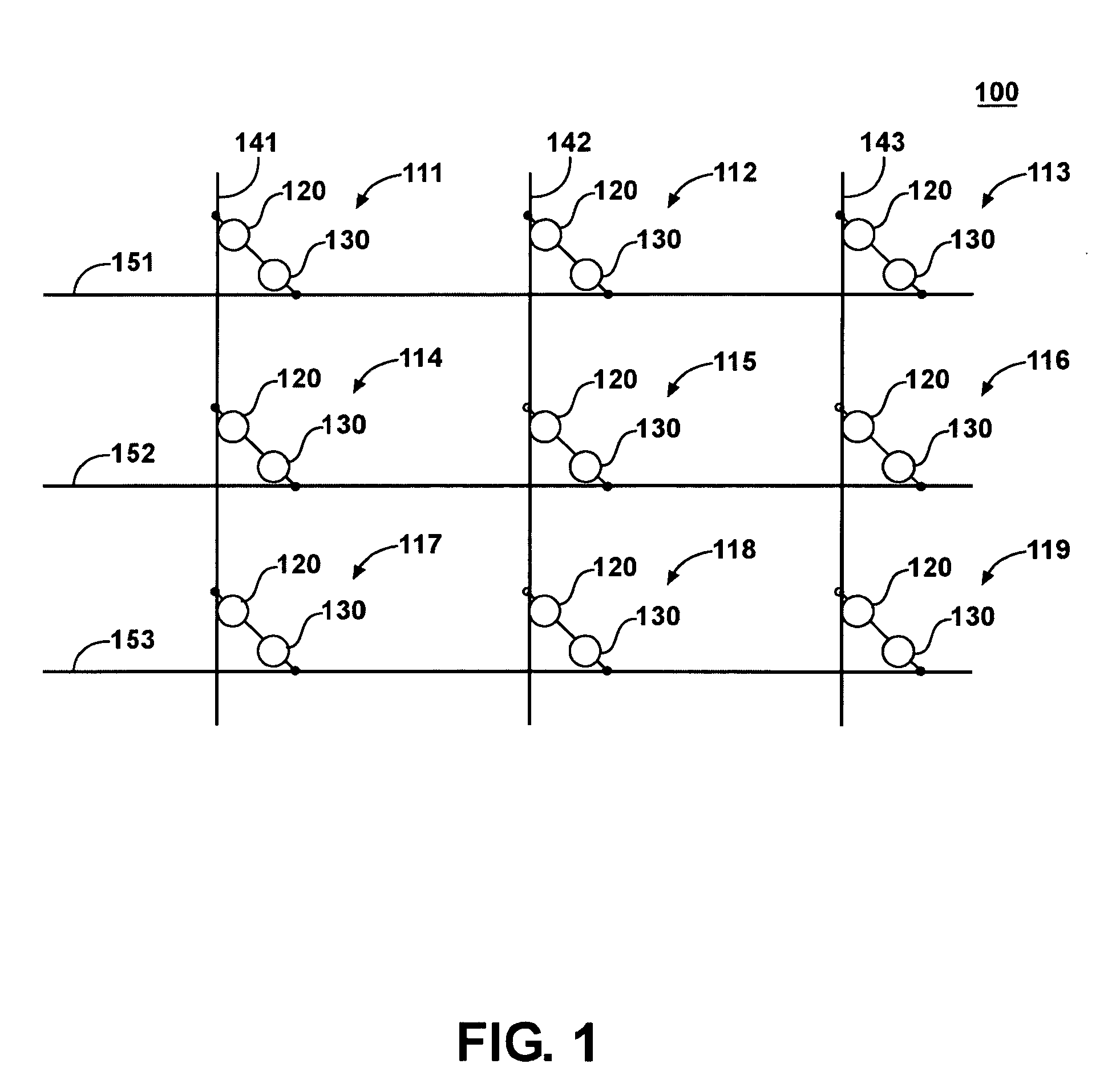
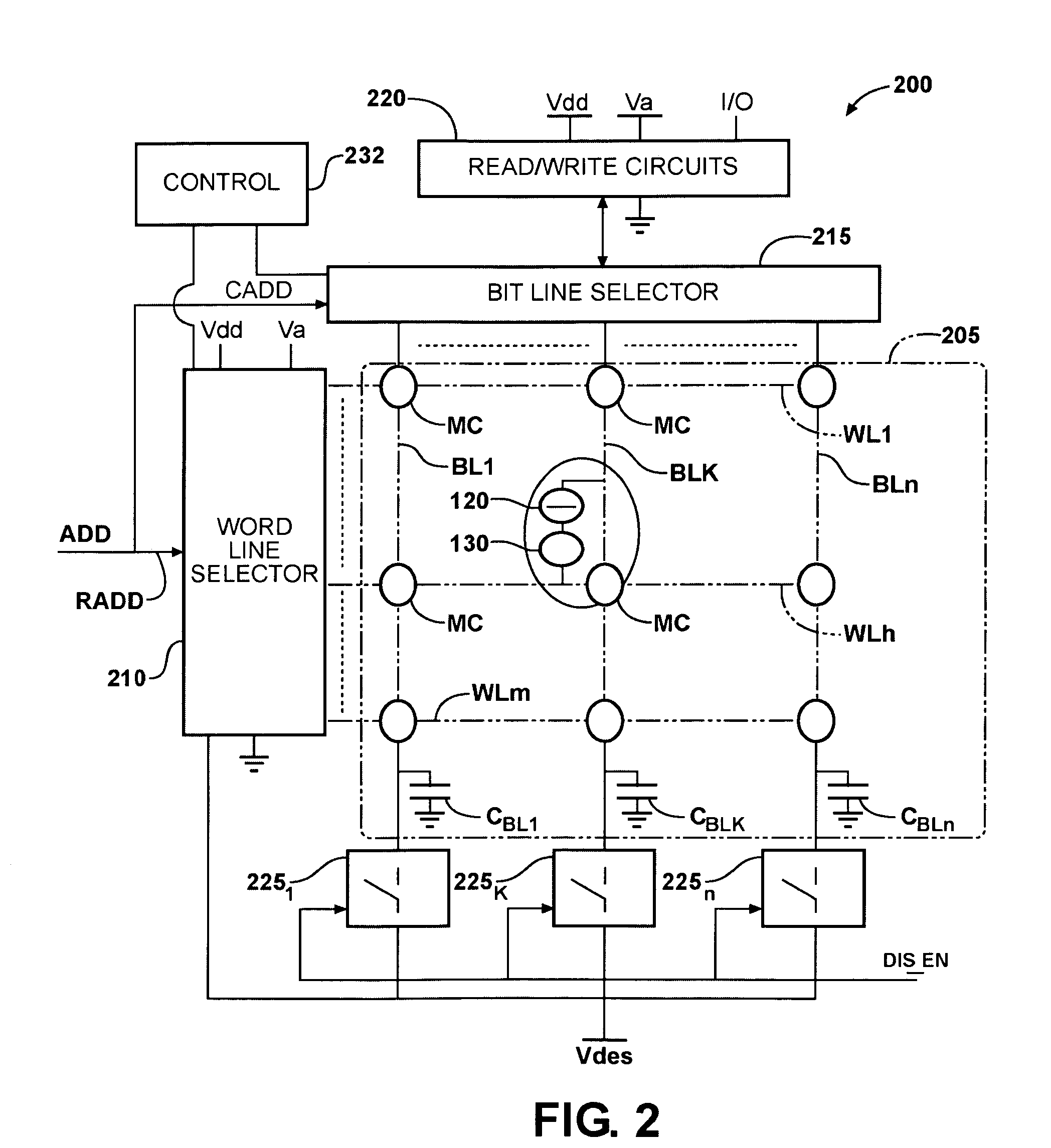
[0030]Although this invention will be described in terms of certain preferred embodiments, other embodiments that are apparent to those of ordinary skill in the art, including embodiments that do not provide all of the benefits and features set forth herein, are also within the scope of this invention. Various structural, logical, process step, chemical, and electrical changes may be made without departing from the spirit or scope of the invention. Polarities and types of devices and supplies may be substituted in a manner that would be apparent to one of reasonable skill in the art. Process descriptions may include flowcharts that illustrate various steps taken in a process. Such flowcharts and accompanying discussion are not meant to be an exhaustive explanation of every step and every procedure in such a process. Rather, they are meant to provide a description with sufficient detail to enable one of ordinary skill in the art to practice and use the invention. In some embodiments,...


PUM


Abstract

A memory includes a programmable resistance array with high ratio of dynamic range to drift coefficient phase change memory devices.

Description

CROSS-REFERENCE TO RELATED APPLICATIONSFIELD OF INVENTION[0001]This invention relates to electronic memory devices.BACKGROUND OF THE INVENTION[0002]As electronic memories approach limits beyond which they will no longer be able to produce the density / cost / performance improvements so famously set forth in Moore's law, a host of memory technologies are being investigated as potential replacements for conventional silicon complementary metal oxide semiconductor (CMOS) integrated circuit memories. Among the technologies being investigated are programmable resistance technologies, such as phase change memory technologies. Phase-change memory arrays are based upon memory elements that switch among two material phases, or gradations thereof, to exhibit corresponding distinct electrical characteristics. Alloys of elements of group VI of the periodic table, such as Te, S or Se, referred to as chalcogenides or chalcogenic materials, can be used advantageously in phase change memory cells. In ...

Claims


Application Information

Patent Timeline
Patent Type & Authority Applications(United States)
IPC IPC(8): G11C11/00H01L21/00G11C11/416
CPCG11C11/56G11C11/5678G11C13/0004G11C13/0035
Inventor LOWREY, TYLERSCHELL, CARLCZUBATYJ, WALLYHUDGENS, STEVEMAIMON, JONFOURNIER, JEFFHENNESSEY, MIKESPALL, ED
Owner OVONYX MEMORY TECH LLC
Why Eureka
Try Eureka