Atomic layer deposition apparatus

a technology of atomic layer and deposition apparatus, which is applied in the direction of chemical vapor deposition coating, coating, coating process, etc., can solve the problems of reducing throughput and productivity, time required for replacing buffer and supplementing substrate, and reducing the time required for loading/unloading and transporting the 12 pieces of substrate, so as to reduce the time required for transporting and prevent the effect of time delay

Active Publication Date: 2010-07-29
K C TECH
View PDF21 Cites 380 Cited by
  • Summary
  • Abstract
  • Description
  • Claims
  • Application Information

AI Technical Summary

Benefits of technology

[0031]As described above, according to exemplary embodiments, a transfer robot including a plurality of handling arms may be provided to simultaneously transport and load / unload at least two substrates, thereby effectively reducing a time required for transporting and loading / unloading the substrate, and preventing a time delay occurring in the transfer robot.
[0032]Also, according to exemplary embodiments, a buffer may be provided to prevent some substrates from remaining on a load port when loading / unloading the substrates due to a number of substrates accommodated in the load port and a number of substrates simultaneously accommodated in a process chamber, and to prevent a process from being delayed due to treatment of extra substrates.

Problems solved by technology

However, in the existing ALD apparatus, since one transfer robot serves to load / unload and transport the substrate, a time required for loading / unloading and transporting the 12 pieces of the substrate may be great.
When a time is delayed in the transfer robot while loading / unloading and transporting the substrate, a time delay may occur during the deposition process to thereby reduce throughput and productivity.
As a result, a time required for replacing the buffer and supplementing the substrate may be needed due to treatment of the extra substrates.

Method used


Image

  • Atomic layer deposition apparatus
  • Atomic layer deposition apparatus
  • Atomic layer deposition apparatus

Examples


Embodiment Construction

[0048]Reference will now be made in detail to exemplary embodiments, examples of which are illustrated in the accompanying drawings, wherein like reference numerals refer to the like elements throughout. Exemplary embodiments are described below to explain the present disclosure by referring to the figures.

[0049]Hereinafter, an atomic layer deposition apparatus according to exemplary embodiments will be described in detail with reference to FIGS. 1 to 14.

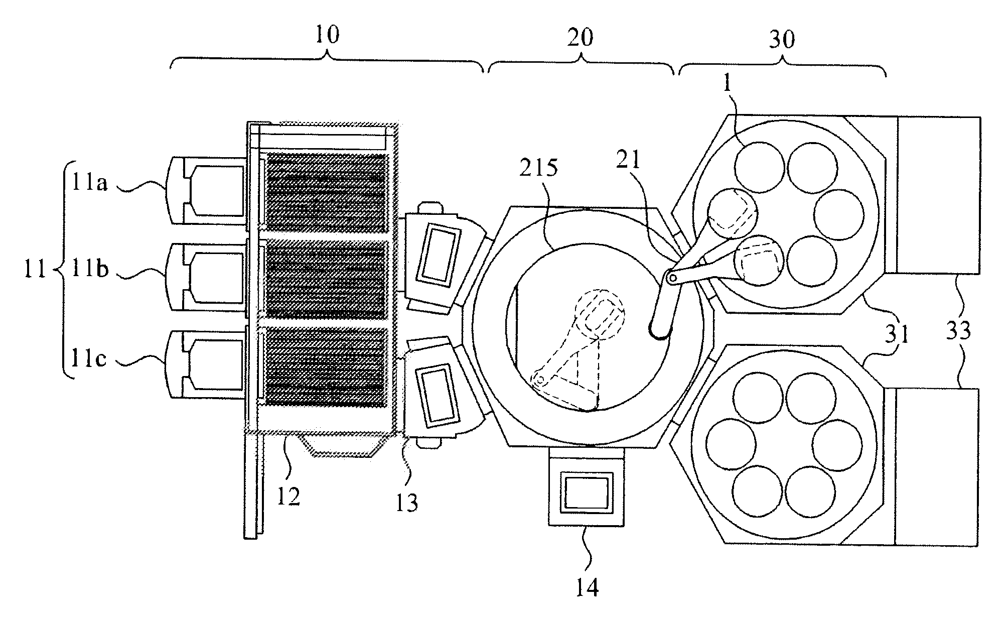
[0050]An entire system of the atomic layer deposition apparatus will be described in detail with reference to FIG. 1. FIG. 1 is a plane view illustrating an entire system of an atomic layer deposition apparatus according to an exemplary embodiment.

[0051]Referring to FIG. 1, the atomic layer deposition apparatus includes a loading / unloading module 10 for loading / unloading a substrate 1 on the atomic layer deposition apparatus, a process module 30 where a deposition process of an atomic layer is performed, and a transfer module 20 for...


PUM

PropertyMeasurementUnit
internal pressureaaaaaaaaaa
diameteraaaaaaaaaa
sizeaaaaaaaaaa

Abstract

An atomic deposition apparatus is provided for simultaneously loading / unloading a plurality of substrates. The atomic deposition apparatus which may load / unload the plurality of substrates when transmitting the plurality of substrates to a process module, includes a loading / unloading module for loading / unloading a substrate, a process module including a plurality of process chambers for simultaneously receiving a plurality of substrates and performing a deposition process, each of the plurality of process chambers including a gas spraying unit having an exhaust portion by which an exhaust gas is drawn in from inside the process chamber and the drawn in gas is exhausted above the process chamber, and a transfer module including a transfer robot provided between the loading / unloading module and the process module, the transfer robot being adopted for simultaneously holding the plurality of substrates while transporting the substrate.

Description

CROSS-REFERENCE TO RELATED APPLICATIONS[0001]This application claims the benefit of Korean Patent Applications No. 10-2008-0135963, filed on Dec. 29, 2008, and No. 10-2009-0047519, filed on May 29, 2009 in the Korean Intellectual Property Office, the disclosures of which are incorporated herein by reference.BACKGROUND[0002]1. Field[0003]Exemplary embodiments relate to an atomic layer deposition apparatus, and more particularly, to an atomic layer deposition apparatus that may simultaneously load and unload a plurality of substrates to improve a throughput.[0004]2. Description of the Related Art[0005]In general, to deposit a thin film with a predetermined thickness on a substrate such as a semiconductor substrate, a glass, and the like, there may be used a method of fabricating the thin film utilizing a physical vapor deposition (PVD) using physical collision such as sputtering, a chemical vapor deposition (CVD) using chemical reaction, and the like.[0006]As a design rule of a semico...

Claims


Application Information

Patent Timeline
Patent Type & Authority Applications(United States)
IPC IPC(8): C23C16/46C23C16/00C23C16/458
CPCC23C16/45546H01L21/67742H01L21/67754H01L21/68764H01L21/68771
Inventor SHIN, IN CHULKIM, KYUNG JOON
Owner K C TECH
Why Eureka
Try Eureka